74ALVC16373MTDX Fairchild Semiconductor, 74ALVC16373MTDX Datasheet

IC LATCH TRANSP 16BIT LV 48TSSOP

74ALVC16373MTDX

Manufacturer Part Number
74ALVC16373MTDX
Description
IC LATCH TRANSP 16BIT LV 48TSSOP
Manufacturer
Fairchild Semiconductor
Series
74ALVCr
Datasheet

Specifications of 74ALVC16373MTDX

Logic Type
D-Type Transparent Latch
Circuit
8:8
Output Type
Tri-State
Voltage - Supply
1.65 V ~ 3.6 V
Independent Circuits
2
Delay Time - Propagation
1ns
Current - Output High, Low
24mA, 24mA
Operating Temperature
-40°C ~ 85°C
Mounting Type
Surface Mount
Package / Case
48-TSSOP
Lead Free Status / RoHS Status
Lead free / RoHS Compliant

Available stocks

Company
Part Number
Manufacturer
Quantity
Price
Part Number:
74ALVC16373MTDX
Manufacturer:
FAIRCHILD
Quantity:
673
© 2005 Fairchild Semiconductor Corporation
74ALVC16373GX
(Note 2)
74ALVC16373MTD
(Note 3)
74ALVC16373
Low Voltage 16-Bit Transparent Latch
with 3.6V Tolerant Inputs and Outputs
General Description
The ALVC16373 contains sixteen non-inverting latches
with 3-STATE outputs and is intended for bus oriented
applications. The device is byte controlled. The flip-flops
appear to be transparent to the data when the Latch
Enable (LE) is HIGH. When LE is LOW, the data that meets
the setup time is latched. Data appears on the bus when
the Output Enable (OE) is LOW. When OE is HIGH, the
outputs are in a high impedance state.
The 74ALVC16373 is designed for low voltage (1.1V to
3.6V) V
The 74ALVC16373 is fabricated with an advanced CMOS
technology to achieve high speed operation while maintain-
ing low CMOS power dissipation.
Ordering Code:
Note 2: BGA package available in Tape and Reel only.
Note 3: Devices also available in Tape and Reel. Specify by appending suffix letter “X” to the ordering code.
Logic Symbol
Order Number
CC
applications with I/O compatibility up to 3.6V.
Package Number
(Preliminary)
BGA54A
MTD48
54-Ball Fine-Pitch Ball Grid Array (FBGA), JEDEC MO-205, 5.5mm Wide
[TAPE and REEL]
48-Lead Thin Shrink Small Outline Package (TSSOP), JEDEC MO-153, 6.1mm Wide
DS500687
Features
Note 1: To ensure the high-impedance state during power up or power
down, OE should be tied to V
value of the resistor is determined by the current-sourcing capability of the
driver.
1.1V to 3.6V V
3.6V tolerant inputs and outputs
t
Power-off high impedance inputs and outputs
Support live insertion and withdrawal (Note 1)
Uses patented noise/EMI reduction circuitry
Latchup conforms to JEDEC JED78
ESD performance:
Also packaged in plastic Fine-Pitch Ball Grid Array
(FBGA) (Preliminary)
PD
3.5 ns max for 3.0V to 3.6V V
3.9 ns max for 2.3V to 2.7V V
6.8 ns max for 1.65V to 1.95V V
Human body model
Machine model
(I
n
Package Description
to O
n
)
CC
supply operation
!
200V
CC
!
2000V
through a pull-up resistor; the minimum
October 2001
Revised May 2005
CC
CC
CC
www.fairchildsemi.com

Related parts for 74ALVC16373MTDX

74ALVC16373MTDX Summary of contents

Page 1

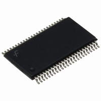
... Thin Shrink Small Outline Package (TSSOP), JEDEC MO-153, 6.1mm Wide (Note 3) Note 2: BGA package available in Tape and Reel only. Note 3: Devices also available in Tape and Reel. Specify by appending suffix letter “X” to the ordering code. Logic Symbol © 2005 Fairchild Semiconductor Corporation Features 1.1V to 3.6V V supply operation CC 3 ...

Page 2

Connection Diagrams Pin Assignment for TSSOP Pin Assignment for FBGA (Top Thru View) www.fairchildsemi.com Pin Descriptions Pin Names Description OE Output Enable Input (Active LOW Latch Enable Input n I –I Inputs –O Outputs 0 ...

Page 3

Functional Description The 74ALVC16373 contains sixteen edge D-type latches with 3-STATE outputs. The device is byte controlled with each byte functioning identically, but independent of the other. Control pins can be shorted together to obtain full 16-bit operation. The following ...

Page 4

Absolute Maximum Ratings Supply Voltage ( Input Voltage ( Output Voltage (V ) (Note 5) 0. Input Diode Current ( Output Diode Current ...

Page 5

AC Electrical Characteristics Symbol Parameter V CC Min Propagation Delay PHL PLH 1.3 Bus to Bus Propagation Delay PHL PLH 1 Bus Output Enable Time 1.3 PZL PZH t ...

Page 6

AC Loading and Waveforms FIGURE 1. AC Test Circuit (Input Characteristics: f Symbol r 3.3V 0. FIGURE 2. Waveform ...

Page 7

Physical Dimensions inches (millimeters) unless otherwise noted 54-Ball Fine-Pitch Ball Grid Array (FBGA), JEDEC MO-205, 5.5mm Wide Package Number BGA54A (Preliminary) 7 www.fairchildsemi.com ...

Page 8

Physical Dimensions inches (millimeters) unless otherwise noted (Continued) 48-Lead Thin Shrink Small Outline Package (TSSOP), JEDEC MO-153, 6.1mm Wide Fairchild does not assume any responsibility for use of any circuitry described, no circuit patent licenses are implied and Fairchild reserves ...

Related keywords