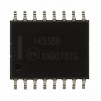
MC14538BDWR2G ON Semiconductor, MC14538BDWR2G Datasheet - Page 5

MC14538BDWR2G
Manufacturer Part Number
MC14538BDWR2G
Description
IC MULTIVIBRATR DUAL CMOS 16SOIC
Manufacturer
ON Semiconductor
Series
4000Br
Datasheet
1.MC14538BCPG.pdf
(12 pages)
Specifications of MC14538BDWR2G
Logic Type
Monostable
Independent Circuits
2
Schmitt Trigger Input
No
Propagation Delay
95ns
Current - Output High, Low
8.8mA, 8.8mA
Voltage - Supply
3 V ~ 18 V
Operating Temperature
-55°C ~ 125°C
Mounting Type
Surface Mount
Package / Case
16-SOIC (0.300", 7.5mm Width)
Elements Per Chip
2
Logic Family
4000
Input Bias Current (max)
0.7 mA
Propagation Delay Time
600 ns, 300 ns, 220 ns
High Level Output Current
- 4.2 mA
Low Level Output Current
4.2 mA
Supply Voltage (max)
18 V
Supply Voltage (min)
3 V
Maximum Operating Temperature
+ 125 C
Minimum Operating Temperature
- 55 C
Mounting Style
SMD/SMT
Operating Supply Voltage
3.3 V, 5 V, 9 V, 12 V
Quiescent Current
700nA
Number Of Elements
2
Operating Temperature Classification
Military
Operating Supply Voltage (max)
18V
Operating Supply Voltage (typ)
3.3/5/9/12/15V
Operating Temperature (min)
-55C
Operating Temperature (max)
125C
Technology
CMOS
Abs. Propagation Delay Time
600ns
Operating Supply Voltage (min)
3V
Lead Free Status / RoHS Status
Lead free / RoHS Compliant
Other names
MC14538BDWR2GOS
MC14538BDWR2GOS
MC14538BDWR2GOSTR
MC14538BDWR2GOS
MC14538BDWR2GOSTR
Available stocks
Company
Part Number
Manufacturer
Quantity
Price
Company:
Part Number:
MC14538BDWR2G
Manufacturer:
TOSHIBA
Quantity:
2 000
Part Number:
MC14538BDWR2G
Manufacturer:
ON/安森美
Quantity:
20 000
GENERATOR
GENERATOR
GENERATOR
PULSE
PULSE
PULSE
V
C
R
DD
V
X
X
in
RESET
V
SS
A
B
2
1
4 (12)
5 (11)
3 (13)
(14)
(15)
V
500 pF
SS
A
B
RESET
A′
B′
RESET′
C
X
R
X
C
A
B
RESET
A′
B′
RESET′
X
V
N1
R
P1
V
C
DD
V
SS
X
X
DD
/R
V
C
X
SS
V
X
V
Figure 2. Power Dissipation Test Circuit and Waveforms
I
D
/R
DD
ref1
R
V
X
X
Q′
Q′
SS
′
Q
Q
C
R
X
X
′
′
Q′
Q′
C
Q
Q
C
+
−
X
0.1 mF
CERAMIC
L
C1
′
V
C
ENABLE
C
SS
L
*C
L
Figure 3. Switching Test Circuit
V
C
L
C
SS
L
= 50 pF
L
Figure 1. Logic Diagram
(1/2 of DevIce Shown)
C
C
L
http://onsemi.com
CONTROL
L
C
MC14538B
V
L
ref2
S
S
Q
R
*Includes capacitance of probes,
NOTE: Switching test waveforms
5
RESET LATCH
wiring, and fixture parasitic.
+
−
C2
ENABLE
for PG1, PG2, PG3 are shown
In Figure 4.
V
in
20 ns
t
T, t
t
T, t
t
t
PLH
PLH
PLH(R)
WH
Q
WH
WH
R
R
, t
Characteristics
, t
, t
WL
PHL
, t
PHL
, t
, t
WL
WL
PHL(R)
10%
, t
, t
TLH
TLH
90%
INPUT CONNECTIONS
,
, t
, t
NOTE: Pins 1, 8 and 15 must
THL
THL
R
S
OUTPUT
LATCH
,
,
be externally grounded
Q
Q
Reset
PG3
V
V
DD
DD
PG1 =
PG2 =
PG3 =
20 ns
6 (10)
7 (9)
PG1
PG1
V
V
0 V
A
SS
DD
PG2
PG2
V
B
DD


