74VHC221AM Fairchild Semiconductor, 74VHC221AM Datasheet - Page 5
74VHC221AM
Manufacturer Part Number
74VHC221AM
Description
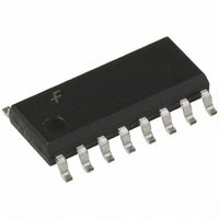
MULTIVIBRATOR DUAL MONO 16SOIC
Manufacturer
Fairchild Semiconductor
Series
74VHCr
Datasheet
1.74VHC221AMTCX.pdf
(12 pages)
Specifications of 74VHC221AM
Logic Type
Monostable
Independent Circuits
2
Schmitt Trigger Input
No
Propagation Delay
8.1ns
Current - Output High, Low
8mA, 8mA
Voltage - Supply
2 V ~ 5.5 V
Operating Temperature
-40°C ~ 85°C
Mounting Type
Surface Mount
Package / Case
16-SOIC (3.9mm Width)
Elements Per Chip
2
Logic Family
VHC
Input Bias Current (max)
0.004 mA
Propagation Delay Time
24.1 ns, 14 ns
High Level Output Current
- 8 mA
Low Level Output Current
8 mA
Supply Voltage (max)
5.5 V
Supply Voltage (min)
2 V
Maximum Operating Temperature
+ 85 C
Minimum Operating Temperature
- 40 C
Mounting Style
SMD/SMT
Operating Supply Voltage
2.5 V, 3.3 V, 5 V
Lead Free Status / RoHS Status
Lead free / RoHS Compliant
Available stocks
Company
Part Number
Manufacturer
Quantity
Price
Company:

Part Number:
74VHC221AM
Manufacturer:
Fairchild Semiconductor
Quantity:
1 816
Company:
Part Number:
74VHC221AMTCX
Manufacturer:
ABOV
Quantity:
26
Company:
Part Number:
74VHC221AMTCX
Manufacturer:
FSC
Quantity:
8 300


©1994 Fairchild Semiconductor Corporation
74VHC221A Rev. 1.2
Absolute Maximum Ratings
Stresses exceeding the absolute maximum ratings may damage the device. The device may not function or be
operable above the recommended operating conditions and stressing the parts to these levels is not recommended.
In addition, extended exposure to stresses above the recommended operating conditions may affect device reliability.
The absolute maximum ratings are stress ratings only.
Recommended Operating Conditions
The Recommended Operating Conditions table defines the conditions for actual device operation. Recommended
operating conditions are specified to ensure optimal performance to the datasheet specifications. Fairchild does not
recommend exceeding them or designing to absolute maximum ratings.
Notes:
1. Unused inputs must be held HIGH or LOW. They may not float.
2. The maximum allowable values of Cx and Rx are a function of the leakage of capacitor Cx, the leakage of the device,
Symbol
Symbol
and leakage due to board layout and surface resistance.
Susceptibility to externally induced noise signals may occur for Rx
V
T
V
T
I
V
V
t
V
V
I
OUT
I
OUT
OPR
r
OUT
I
STG
T
OK
CC
CC
, t
CC
IK
IN
IN
L
f
External Capacitor, Cx
External Resistor, Rx
Supply Voltage
Input Voltage
Output Voltage
Operating Temperature
Input Rise and Fall Time (CLR only)
Supply Voltage
DC Input Voltage
DC Output Voltage
Input Diode Current
Output Diode Current
DC Output Current
DC V
Storage Temperature
Lead Temperature (Soldering, 10 seconds)
V
V
CC
CC
CC
/ GND Current
3.3V ± 0.3V
5.0V ± 0.5V
Parameter
Parameter
(1)
5
1 M .
1k
–0.5V to V
5k
Rating
Rating
No Limitation
–65°C to +150°C
0ns/V
(2)
–40°C to +85°C
(2)
0ns/V
–0.5V to +7.0V
–0.5V to +7.0V
2.0V to +5.5V
(V
(V
www.fairchildsemi.com
0V to +5.5V
CC
CC
0V to V
CC
100ns/V
20ns/V
–20mA
±20mA
±25mA
±50mA
+ 0.5V
260°C
2.0V)
3.0V)
(2)
CC
F
Related parts for 74VHC221AM
Image
Part Number
Description
Manufacturer
Datasheet
Request
R

Part Number:
Description:
Fairchild Semiconductor [IGBT MODULE]
Manufacturer:
Fairchild Semiconductor
Datasheet:

Part Number:
Description:
Discrete Semiconductor Modules
Manufacturer:
Fairchild Semiconductor
Part Number:
Description:
Discrete Semiconductor Modules
Manufacturer:
Fairchild Semiconductor
Part Number:
Description:
This N-Channel MOSFET is produced using Fairchild Semiconductor’s advanced Power Trench® process
Manufacturer:
Fairchild Semiconductor
Datasheet:
Part Number:
Description:
This N-Channel MOSFET is produced using Fairchild Semiconductor’s advanced Power Trench® process
Manufacturer:
Fairchild Semiconductor
Datasheet:
Part Number:
Description:
This N-Channel MOSFET is produced using Fairchild Semiconductor’s advanced PowerTrench® process
Manufacturer:
Fairchild Semiconductor
Datasheet:
Part Number:
Description:
This N-Channel MOSFET is produced using Fairchild Semiconductor’s advanced PowerTrench® process
Manufacturer:
Fairchild Semiconductor
Datasheet:
Part Number:
Description:
This N-Channel MOSFET is produced using Fairchild Semiconductor’s advanced Power Trench® process
Manufacturer:
Fairchild Semiconductor
Datasheet:
Part Number:
Description:
This N-Channel logic Level MOSFETs are produced using Fairchild Semiconductor‘s advanced Power Trench® process that has been special tailored to minimize the on-state resistance and yet maintain superior switching performance
Manufacturer:
Fairchild Semiconductor
Datasheet:
Part Number:
Description:
This N-Channel MOSFET is produced using Fairchild Semiconductor’s advanced Power Trench® process
Manufacturer:
Fairchild Semiconductor
Datasheet:
Part Number:
Description:
This N-Channel SyncFET™ is produced using Fairchild Semiconductor’s advanced PowerTrench® process
Manufacturer:
Fairchild Semiconductor
Datasheet:
Part Number:
Description:
This N-Channel SyncFET™ is produced using Fairchild Semiconductor’s advanced PowerTrench® process
Manufacturer:
Fairchild Semiconductor
Datasheet:
Part Number:
Description:
This N-Channel SyncFET™ is produced using Fairchild Semiconductor’s advanced PowerTrench® process
Manufacturer:
Fairchild Semiconductor
Datasheet:
Part Number:
Description:
This N-Channel logic Level MOSFETs are produced using Fairchild Semiconductor‘s advanced Power Trench® process that has been special tailored to minimize the on-state resistance and yet maintain superior switching performance
Manufacturer:
Fairchild Semiconductor
Datasheet:
Part Number:
Description:
This N-Channel MOSFET is produced using Fairchild Semiconductor’s advanced Power Trench® process that has been especially tailored to minimize the on-state resistance and yet maintain superior switching performance
Manufacturer:
Fairchild Semiconductor
Datasheet: