MC14094BCPG ON Semiconductor, MC14094BCPG Datasheet

IC SHIFT REGISTER 8STAGE 16-DIP

MC14094BCPG

Manufacturer Part Number
MC14094BCPG
Description
IC SHIFT REGISTER 8STAGE 16-DIP
Manufacturer
ON Semiconductor
Series
4000Br
Type
Not Requiredr
Datasheets

Specifications of MC14094BCPG

Logic Type
Shift Register
Output Type
Standard
Number Of Elements
1
Number Of Bits Per Element
8
Function
Serial to Parallel
Voltage - Supply
3 V ~ 18 V
Operating Temperature
-55°C ~ 125°C
Mounting Type
Through Hole
Package / Case
16-DIP (0.300", 7.62mm)
Technology
CMOS
Number Of Elements
1
Number Of Bits
8
Logic Family
4000
Logical Function
Shift Register
Operating Supply Voltage (typ)
3.3/5/9/12/15V
Package Type
PDIP
Propagation Delay Time
840ns
Operating Temp Range
-55C to 125C
Operating Supply Voltage (min)
3V
Operating Supply Voltage (max)
18V
Operating Temperature Classification
Military
Mounting
Through Hole
Pin Count
16
Counting Sequence
Serial to Serial/Parallel
Number Of Circuits
2
Supply Voltage (max)
18 V
Maximum Operating Temperature
+ 125 C
Minimum Operating Temperature
- 55 C
Mounting Style
Through Hole
Operating Supply Voltage
3 V to 18 V
Circuit Type
Low-Power Schottky
Current, Supply
600 μA
Function Type
8-Stages
Logic Function
Register
Special Features
Tri-State
Temperature, Operating, Range
-55 to +125 °C
Voltage, Supply
3 to 18 VDC
Lead Free Status / RoHS Status
Lead free / RoHS Compliant
Other names
MC14094BCPGOS

Available stocks

Company
Part Number
Manufacturer
Quantity
Price
Part Number:
MC14094BCPG
Manufacturer:
TI
Quantity:
12 400
MC14094B
8−Stage Shift/Store Register
with Three−State Outputs
for each stage and a 3−state output from each latch.
seventh stage to two serial outputs. The Q
high−speed cascaded systems. The Q
following negative clock transition for use in low−speed cascaded
systems.
transition of the strobe input. Data propagates through the latch while
strobe is high.
which are placed in the high−impedance state by a logic Low on
Output Enable.
Features
1. Temperature Derating:
static voltages or electric fields. However, precautions must be taken to avoid
applications of any voltage higher than maximum rated voltages to this
high−impedance circuit. For proper operation, V
to the range V
(e.g., either V
MAXIMUM RATINGS
© Semiconductor Components Industries, LLC, 2005
Symbol
V
I
The MC14094B combines an 8−stage shift register with a data latch
Data is shifted on the positive clock transition and is shifted from the
Data from each stage of the shift register is latched on the negative
Outputs of the eight data latches are controlled by 3−state buffers
in
This device contains protection circuitry to guard against damage due to high
Unused inputs must always be tied to an appropriate logic voltage level
Schottky TTL Load Over the Rated Temperature Range
Negative Clock Transitions
in
3−State Outputs
Capable of Driving Two Low−Power TTL Loads or One Low−Power
Input Diode Protection
Data Latch
Dual Outputs for Data Out on Both Positive and
Useful for Serial−to−Parallel Data Conversion
Pin−for−Pin Compatible with CD4094B
Pb−Free Packages are Available*
V
T
Plastic “P and D/DW” Packages: – 7.0 mW/_C From 65_C To 125_C
P
, V
, I
T
T
stg
DD
A
D
L
out
out
DC Supply Voltage Range
Input or Output Voltage Range
Input or Output Current
Power Dissipation, per Package
Ambient Temperature Range
Storage Temperature Range
Lead Temperature
SS
SS
(DC or Transient)
(DC or Transient) per Pin
(Note 1)
(8−Second Soldering)
or V
v (V
DD
in
). Unused outputs must be left open.
Parameter
or V
(Voltages Referenced to V
out
) v V
DD
.
S
output data is shifted on the
in
and V
S
−0.5 to V
output data is for use in
SS
−0.5 to +18.0
−55 to +125
−65 to +150
out
)
Value
± 10
500
260
should be constrained
DD
+ 0.5
1
Unit
mW
mA
°C
°C
°C
V
V
See detailed ordering and shipping information in the package
dimensions section on page 2 of this data sheet.
*For additional information on our Pb−Free strategy
and soldering details, please download the
ON Semiconductor Soldering and Mounting
Techniques Reference Manual, SOLDERRM/D.
ORDERING INFORMATION
A
WL, L
YY, Y
WW, W
G
CASE 751B
CASE 948F
SOEIAJ−16
TSSOP−16
DT SUFFIX
CASE 648
CASE 966
P SUFFIX
D SUFFIX
F SUFFIX
PDIP−16
SOIC−16
= Assembly Location
= Wafer Lot
= Year
= Work Week
= Pb−Free Indicator
Publication Order Number:
16
1
16
16
1
1
DIAGRAMS
16
MARKING
MC14094BCP
AWLYYWWG
1
MC14094B
AWLYWW
MC14094B/D
14094BG
ALYWG
ALYW
094B
14

Related parts for MC14094BCPG

MC14094BCPG Summary of contents

Page 1

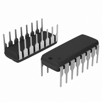
... ORDERING INFORMATION See detailed ordering and shipping information in the package dimensions section on page 2 of this data sheet. *For additional information on our Pb−Free strategy and soldering details, please download the ON Semiconductor Soldering and Mounting Techniques Reference Manual, SOLDERRM/D. Publication Order Number: MC14094B/D 14 ...

Page 2

... Z = High Impedance * At the positive clock edge, information in the 7th shift register stage is transferred to Q8 and Q ORDERING INFORMATION Device MC14094BCP MC14094BCPG MC14094BD MC14094BDG MC14094BDR2 MC14094BDR2G MC14094BDTR2 MC14094BF MC14094BFG MC14094BFEL MC14094BFELG †For information on tape and reel specifications, including part orientation and tape sizes, please refer to our Tape and Reel Packaging Specifications Brochure, BRD8011/D. *This package is inherently Pb− ...

Page 3

ELECTRICAL CHARACTERISTICS Î Î Î Î Î ...

Page 4

SWITCHING CHARACTERISTICS Î Î Î Î Î ...

Page 5

0.25 (0.010) M −A− −T− SEATING PLANE 0.25 (0.010 MC14094B PACKAGE DIMENSIONS PDIP−16 ...

Related keywords