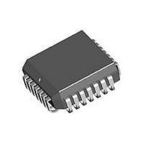
MC10E141FNG ON Semiconductor, MC10E141FNG Datasheet - Page 3

MC10E141FNG
Manufacturer Part Number
MC10E141FNG
Description
IC SHIFT REGISTR 8BIT ECL 28PLCC
Manufacturer
ON Semiconductor
Series
10Er
Datasheet
1.MC100E141FNR2G.pdf
(8 pages)
Specifications of MC10E141FNG
Logic Type
Shift Register
Output Type
Standard
Number Of Elements
1
Number Of Bits Per Element
8
Function
Universal
Voltage - Supply
4.2 V ~ 5.7 V
Operating Temperature
0°C ~ 85°C
Mounting Type
Surface Mount
Package / Case
28-PLCC
Counting Sequence
Serial/Parallel to Parallel
Number Of Circuits
3
Logic Family
10
Propagation Delay Time
0.975 ns
Supply Voltage (max)
5.7 V, 5.7 V
Maximum Operating Temperature
+ 85 C
Minimum Operating Temperature
0 C
Mounting Style
SMD/SMT
Operating Supply Voltage
4.2 V to 5.7 V
Supply Voltage (min)
4.2 V, 4.2 V
Lead Free Status / RoHS Status
Lead free / RoHS Compliant
Other names
MC10E141FNGOS
Available stocks
Company
Part Number
Manufacturer
Quantity
Price
Company:
Part Number:
MC10E141FNG
Manufacturer:
ON Semiconductor
Quantity:
10 000
Stresses exceeding Maximum Ratings may damage the device. Maximum Ratings are stress ratings only. Functional operation above the
Recommended Operating Conditions is not implied. Extended exposure to stresses above the Recommended Operating Conditions may affect
device reliability.
NOTE: Device will meet the specifications after thermal equilibrium has been established when mounted in a test socket or printed circuit
1. Input and output parameters vary 1:1 with V
2. Outputs are terminated through a 50 W resistor to V
Table 4. MAXIMUM RATINGS
Symbol
Table 5. 10E SERIES PECL DC CHARACTERISTICS
V
V
V
I
T
T
q
q
V
T
I
V
V
V
V
I
I
Symbol
out
EE
IH
IL
A
stg
JA
JC
sol
CC
EE
I
EE
OH
OL
IH
IL
board with maintained transverse airflow greater than 500 lfpm. Electrical parameters are guaranteed only over the declared
operating temperature range. Functional operation of the device exceeding these conditions is not implied. Device specification limit
values are applied individually under normal operating conditions and not valid simultaneously.
PECL Mode Power Supply
NECL Mode Power Supply
PECL Mode Input Voltage
NECL Mode Input Voltage
Output Current
Operating Temperature Range
Storage Temperature Range
Thermal Resistance (Junction−to−Ambient)
Thermal Resistance (Junction−to−Case)
PECL Operating Range
NECL Operating Range
Wave Solder
Power Supply Current
Output HIGH Voltage (Note 2)
Output LOW Voltage (Note 2)
Input HIGH Voltage
Input LOW Voltage
Input HIGH Current
Input LOW Current
Characteristic
Parameter
CC
Pb−Free
. V
EE
CC
Pb
can vary −0.46 V / +0.06 V.
3980
3050
3830
3050
Min
0.5
http://onsemi.com
− 2.0 V.
V
V
V
V
Continuous
Surge
0 lfpm
500 lfpm
Standard Board
EE
CC
EE
CC
V
CCx
4070
3210
3995
3285
Condition 1
0°C
Typ
131
= 0 V
= 0 V
0.3
= 0 V
= 0 V
3
= 5.0 V; V
4160
3370
4160
3520
Max
181
150
EE
4020
3050
3870
3050
= 0.0 V (Note 1)
Min
0.5
V
V
PLCC−28
PLCC−28
PLCC−28
I
I
v V
w V
Condition 2
25°C
4105
3210
4030
3285
0.25
Typ
131
CC
EE
4190
3370
4190
3520
Max
181
150
4090
3050
3940
3050
Min
0.3
−65 to +150
−5.7 to −4.2
4.2 to 5.7
0 to +85
22 to 26
Rating
85°C
4185
3227
3302
4110
Typ
131
0.2
63.5
43.5
100
265
265
−8
−6
50
8
6
4280
3405
4280
3555
Max
181
150
°C/W
°C/W
°C/W
Unit
Unit
mA
mA
mA
mV
mV
mV
mV
°C
°C
°C
mA
mA
V
V
V
V
V
V


