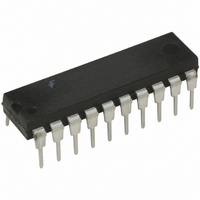
74F323PC Fairchild Semiconductor, 74F323PC Datasheet - Page 2

74F323PC
Manufacturer Part Number
74F323PC
Description
IC REGISTER SHIFT/STOR 20-DIP
Manufacturer
Fairchild Semiconductor
Series
74Fr
Datasheet
1.74F323PC.pdf
(6 pages)
Specifications of 74F323PC
Logic Type
Register, Bidirectional
Output Type
Standard
Number Of Elements
1
Number Of Bits Per Element
8
Function
Universal
Voltage - Supply
4.5 V ~ 5.5 V
Operating Temperature
0°C ~ 70°C
Mounting Type
Through Hole
Package / Case
20-DIP (0.300", 7.62mm)
Lead Free Status / RoHS Status
Lead free / RoHS Compliant
Other names
74F323
www.fairchildsemi.com
Unit Loading/Fan Out
Functional Description
The 74F323 contains eight edge-triggered D-type flip-flops
and the interstage logic necessary to perform synchronous
reset, shift left, shift right, parallel load and hold operations.
The type of operation is determined by S
in the Mode Select Table. All flip-flop outputs are brought
out through 3-STATE buffers to separate I/O pins that also
serve as data inputs in the parallel load mode. Q
are also brought out on other pins for expansion in serial
shifting of longer words.
A LOW signal on SR overrides the Select inputs and allows
the flip-flops to be reset by the next rising edge of CP. All
other state changes are also initiated by the LOW-to-HIGH
CP transition. Inputs can change when the clock is in either
state provided only that the recommended setup and hold
times, relative to the rising edge of CP, are observed.
A HIGH signal on either OE
buffers and puts the I/O pins in the high impedance state.
In this condition the shift, load, hold and reset operations
can still occur. The 3-STATE buffers are also disabled by
HIGH signals on both S
lel load operation.
Mode Select Table
H
L
X
SR S
LOW Voltage Level
H
H
H
H
L
HIGH Voltage Level
Immaterial
LOW-to-HIGH transition
Pin Names
Inputs
X
H
H
L
L
CP
DS
DS
S
SR
OE
I/O
Q
1
0,
0,
0
0
7
1,
S
Q
S
–I/O
X
H
H
L
L
1
OE
0
7
7
CP
2
X Hold
Synchronous Reset; Q
Parallel Load; I/O
Shift Right; DS
Shift Left; DS
Clock Pulse Input (Active Rising Edge)
Serial Data Input for Right Shift
Serial Data Input for Left Shift
Mode Select Inputs
Synchronous Reset Input (Active LOW)
3-STATE Output Enable Inputs (Active LOW)
Multiplexed Parallel Data Inputs
3-STATE Parallel Data Outputs
Serial Outputs
0
and S
1
or OE
1
in preparation for a paral-
Response
7
2
0
disables the 3-STATE
n
Q
0
Description
Q
7,
and S
0,
Q
Q
0
Q
7
–Q
n
0
1
7
as shown
Q
0
Q
6,
and Q
LOW
1,
etc.
etc.
7
2
Logic Diagram
Please note that this diagram is provided only for the understanding of logic
operations and should not be used to estimate propagation delays.
150/40 (33.3)
HIGH/LOW
3.5/1.083
50/33.3
1.0/1.0
1.0/1.0
1.0/1.0
1.0/2.0
1.0/1.0
1.0/1.0
U.L.
3 mA/24 mA (20 mA)
70 A/ 0.65 mA
Output I
20 A/ 0.6 mA
20 A/ 0.6 mA
20 A/ 0.6 mA
20 A/ 1.2 mA
20 A/ 0.6 mA
20 A/ 0.6 mA
Input I
1 mA/20 mA
IH
OH
/I
/I
IL
OL


