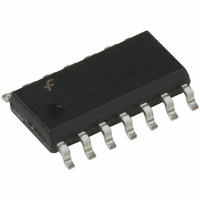
CD4016BCM Fairchild Semiconductor, CD4016BCM Datasheet - Page 2

CD4016BCM
Manufacturer Part Number
CD4016BCM
Description
IC SWITCH BILATERAL QUAD 14-SOIC
Manufacturer
Fairchild Semiconductor
Series
4000Br
Type
Bilateral, FET Switchesr
Datasheet
1.CD4016BCM.pdf
(9 pages)
Specifications of CD4016BCM
Circuit
1 x 1:1
Independent Circuits
4
Voltage Supply Source
Dual Supply
Voltage - Supply
3 V ~ 15 V
Operating Temperature
-55°C ~ 125°C
Mounting Type
Surface Mount
Package / Case
14-SOIC (3.9mm Width), 14-SOL
Switch Configuration
SPST
On Resistance (max)
2000 Ohms
On Time (max)
50 ns
Off Time (max)
40 ns
Supply Voltage (max)
15 V
Supply Voltage (min)
3 V
Maximum Power Dissipation
500 mW
Maximum Operating Temperature
+ 125 C
Mounting Style
SMD/SMT
Minimum Operating Temperature
- 55 C
Propagation Delay Time
100 ns
Analog Switch Type
SPST
No. Of Channels
4
Bandwidth
40MHz
On State Resistance Max
850ohm
Turn Off Time
10ns
Turn On Time
17ns
Supply Voltage Range
3V To 15V
Rohs Compliant
Yes
Lead Free Status / RoHS Status
Contains lead / RoHS non-compliant
Current - Output High, Low
-
Lead Free Status / Rohs Status
Lead free / RoHS Compliant
Available stocks
Company
Part Number
Manufacturer
Quantity
Price
Company:
Part Number:
CD4016BCM
Manufacturer:
SAMSUNG
Quantity:
5
Part Number:
CD4016BCMX
Manufacturer:
FAIRCHILD/ن»™ç«¥
Quantity:
20 000
www.fairchildsemi.com
I
Signal Inputs and Outputs
R
I
Control Inputs
V
V
I
DD
IS
IN
Absolute Maximum Ratings
(Note 2)
DC Electrical Characteristics
Symbol
Note 3: If the switch input is held at V
levels. If the analog switch input is connected to V
current, and still maintain a V
R
ILC
IHC
ON
V
V
T
Power Dissipation (P
Lead Temperature
ON
S
DD
IN
Dual-In-Line
Small Outline
(Soldering, 10 seconds)
Storage Temperature Range
Input Voltage
Supply Voltage
Quiescent Device
Current
“ON” Resistance
Between any 2 of
4 Switches
(In Same Package)
Input or Output
Leakage
Switch “OFF”
LOW Level Input
Voltage
HIGH Level Input
Voltage
Input Current
“ON” Resistance
Parameter
D
OL
)
“B” series. These currents are shown in Table 1.
DD
, V
IHC
V
V
V
R
V
V
V
R
V
V
V
R
V
V
V
V
V
V
V
V
I
V
V
V
V
V
V
(Note 3) and Table 1
V
V
V
IS
DD
DD
DD
L
C
DD
DD
L
C
DD
DD
L
C
DD
DD
C
IS
OS
IS
OS
DD
DD
DD
DD
DD
DD
CC
DD
DD
is the control input level that will cause the switch output to meet the standard “B” series V
10k to (V
10k to (V
10k to (V
V
V
V
0, V
0V or 15V,
V
SS
10 A
5V, V
10V, V
15V, V
10V
15V
10V, V
15V, V
10V
15V
15V or 0V
V
5V
10V
15V
5V
10V
15V
V
V
V
0.5V to V
DD
DD
DD
SS
DD
SS
IS
C
, V
DD
, V
, V
65 C to
and V
IHC
and V
V
IN
IS
IS
V
15V
IN
IN
IS
IS
SS
Conditions
(Note 1)
0.5V to 18V
SS
is the control input level — which allows the switch to sink standard “B” series |I
15V
DD
DD
DD
V
V
V
DD
(Note 2)
4.75 to 5.25V
7.25 to 7.75V
SS
V
V
DD
DD
SS
SS
DD
DD
700 mW
500 mW
V
or V
V
V
to V
or V
150 C
260 C
or V
or V
SS
SS
SS
0.5V
)/2
DD
)/2
)/2
DD
SS
SS
SS
2
Recommended Operating
Conditions
Note 1: “Absolute Maximum Ratings” are those values beyond which the
safety of the device cannot be guaranteed. They are not meant to imply
that the devices should be operated at these limits. The tables of “Recom-
mended Operating Conditions” and “Electrical Characteristics” provide con-
ditions for actual device operation.
Note 2: V
V
V
T
A
DD
IN
Operating Temperature Range
Input Voltage
Supply Voltage
11.0
Min
3.5
7.0
SS
55 C
0V unless otherwise specified.
1870
Max
0.25
600
360
775
0.5
1.0
0.9
0.9
0.9
0.1
50
(Note 2)
11.0
Min
3.5
7.0
25 C
0.01
0.01
0.01
Typ
250
200
850
400
10
15
10
0.1
5
2000
Max
0.25
660
400
850
0.5
1.0
0.7
0.7
0.7
0.1
50
Min
11.0
3.5
7.0
55 C to 125 C
OH
125 C
OH
and I
|, HIGH level
2600
1230
Max
3V to 15V
0V to V
960
600
7.5
0.5
0.5
0.5
15
30
500
1.0
OH
output
Units
DD
nA
V
V
V
V
V
V
A
A
A
A


