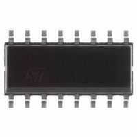
74LCX157MTR STMicroelectronics, 74LCX157MTR Datasheet

74LCX157MTR
Specifications of 74LCX157MTR
Related parts for 74LCX157MTR
74LCX157MTR Summary of contents
Page 1
... Latch-up performance exceeds 500mA (JESD 17) ■ ESD performance: – HBM > 2000V (MIL STD 883 method 3015); MM > 200V Order codes Part number 74LCX157MTR 74LCX157TTR February 2007 Low voltage CMOS Quad 2 channel multiplexer = Description The 74LCX157 is a low voltage CMOS Quad 2 ...
Page 2
Contents Contents 1 Logic symbols and I/O equivalent circuit . . . . . . . . . . . . . . . . . . . . . . . . 3 2 Pin settings . . . ...
Page 3
Logic symbols and I/O equivalent circuit Figure 1. IEC logic symbols Figure 2. Input and output equivalent circuit Logic symbols and I/O equivalent circuit 3/17 ...
Page 4
Pin settings 2 Pin settings 2.1 Pin connection Figure 3. Pin connection (top through view) 2.2 Pin description Table 1. Pin description Pin N° 11 10 ...
Page 5
Truth table Table 2. Truth table STROBE Note not care 2.4 Logic diagram Figure 4. Logic diagram Note: This logic diagram has not to be used to estimate propagation delays ...
Page 6
... STMicroelectronics sure program and other relevant quality documents. Table 3. Absolute maximum ratings ...
Page 7
Electrical characteristics Table 5. DC specifications Symbol V High level input voltage IH V Low level input voltage IL V High level output voltage OH V Low level output voltage OL I Input leakage current I Power OFF ...
Page 8
Electrical characteristics Table 7. AC electrical characteristics Symbol Parameter Propagation delay t t PLH PHL time Propagation delay t t PLH PHL time SELECT Output to output OSLH t skew time OSHL 1. ...
Page 9
Test circuit Figure 5. Test circuit C = 50pF or equivalent (includes jig and probe capacitance) L Ω 500 or equivalent pulse generator (typically 50 T OUT Ω ) Test circuit ...
Page 10
Waveforms 6 Waveforms Figure 6. Propagation delay for inverting outputs (f = 1MHz; 50% duty cycle) Figure 7. Propagation delay for non-inverting outputs (f = 1MHz; 50% duty cycle) 10/17 74LCX157 ...
Page 11
Package mechanical data In order to meet environmental requirements, ST offers these devices in ECOPACK® packages. These packages have a Lead-free second level interconnect . The category of second level interconnect is marked on the package and on ...
Page 12
Package mechanical data DIM 12/17 SO-16 MECHANICAL DATA mm. MIN. TYP MAX. 1.75 0.1 0.25 1.64 0.35 0.46 0.19 0.25 0.5 9.8 10 5.8 ...
Page 13
DIM PIN 1 IDENTIFICATION TSSOP16 MECHANICAL DATA mm. MIN. TYP MAX. 1.2 0.05 0.15 0.8 1 1.05 0.19 0.30 0.09 0.20 4.9 5 5.1 6.2 6.4 ...
Page 14
Package mechanical data DIM 14/17 Tape & Reel SO-16 MECHANICAL DATA mm. MIN. TYP MAX. 330 12.8 13.2 20.2 60 22.4 6.45 6.65 10.3 10.5 2.1 2.3 3.9 4.1 7.9 ...
Page 15
DIM Tape & Reel TSSOP16 MECHANICAL DATA mm. MIN. TYP MAX. 330 12.8 13.2 20.2 60 22.4 6.7 6.9 5.3 5.5 1.6 1.8 3.9 4.1 7.9 8.1 Package mechanical ...
Page 16
Revision history 8 Revision history Table 9. Revision history Date 15-Sep-2004 06-Feb-2007 16/17 Revision 5 Ordering Codes Revision - pag Document reformatted, temperature ranges updated 74LCX157 Changes ...
Page 17
... Information in this document is provided solely in connection with ST products. STMicroelectronics NV and its subsidiaries (“ST”) reserve the right to make changes, corrections, modifications or improvements, to this document, and the products and services described herein at any time, without notice. All ST products are sold pursuant to ST’s terms and conditions of sale. ...


