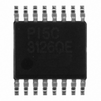
PI5C3126QE Pericom Semiconductor, PI5C3126QE Datasheet - Page 3

PI5C3126QE
Manufacturer Part Number
PI5C3126QE
Description
IC BUS SWITCH 4BIT 16-QSOP
Manufacturer
Pericom Semiconductor
Type
Bus Switchr
Datasheet
1.PI5C3126QE.pdf
(6 pages)
Specifications of PI5C3126QE
Circuit
1 x 1:1
Independent Circuits
4
Voltage Supply Source
Single Supply
Operating Temperature
-40°C ~ 85°C
Mounting Type
Surface Mount
Package / Case
16-QSOP
Number Of Bits
4
Number Of Elements
4
Technology
CMOS
High Level Output Current
-120mA
Low Level Output Current
120mA
Propagation Delay Time
5.4ns
Package Type
QSOP
Operating Temp Range
-40C to 85C
Operating Temperature Classification
Industrial
Operating Supply Voltage (min)
4.5V
Operating Supply Voltage (typ)
5V
Operating Supply Voltage (max)
5.5V
Quiescent Current
3uA
Pin Count
16
Mounting
Surface Mount
Lead Free Status / RoHS Status
Lead free / RoHS Compliant
Voltage - Supply
-
Current - Output High, Low
-
Lead Free Status / Rohs Status
Compliant
Available stocks
Company
Part Number
Manufacturer
Quantity
Price
Part Number:
PI5C3126QE
Manufacturer:
PERICOM
Quantity:
20 000
Company:
Part Number:
PI5C3126QEX
Manufacturer:
NEC
Quantity:
195
Part Number:
PI5C3126QEX
Manufacturer:
PERICOM
Quantity:
20 000
DC Electrical Characteristics
Notes:
1.
2.
3.
4.
Capacitance
Notes:
1.
Power Supply Characteristics
Notes:
1.
2.
3.
4.
Parameters
Parameters
Parameters
For Max. or Min. conditions, use appropriate value specified under Electrical Characteristics for the applicable device type.
Typical values are at V
Not more than one output should be shorted at one time. Duration of the test should not exceed one second.
Measured by the voltage drop between A and B pin at indicated current through the switch. ON resistance is determined by the lower of the
voltages on the two (A, B) pins.
This parameter is determined by device characterization but is not production tested.
For Max. or Min. conditions, use appropriate value specified under Electrical Characteristics for the applicable device.
Typical values are at V
Per TTL driven input (V
This current applies to the control inputs only and represent the current required to switch internal capacitance at the specified frequency.
The A and B inputs generate no significant AC or DC currents as they transition. This parameter is not tested, but is guaranteed by design.
I
R
ΔI
I
V
V
V
I
OZH
V
I
I
I
CCD
OS
IH
CC
IL
ON
IH
IK
IL
06-0238
H
CC
C
C
C
OFF
ON
IN
(T
(1)
Input HIGH Voltage
Input LOW Voltage
Input HIGH Current
Input LOW Current
High Impedance Output Current
Clamp Diode Voltage
Short Circuit Current
Input Hysteresis at Control Pins
Switch On-Resistance
Quiescent Power
Supply Current
Supply Current per
Input @ TTL HIGH
Supply Current per
Input per MHz
A
= 25°C, f = 1 MHz)
Input Capacitance
A/B Capacitance, Switch Off
A/B Capacitance, Switch On
CC
Description
CC
IN
Description
= 5.0V, T
= 5.0V, +25°C ambient.
= 3.4V, control inputs only); A and B pins do not contribute to I
(4)
A
(Over the Operating Range, T
(3)
= 25°C ambient and maximum loading.
(4)
Description
V
V
V
A and B Pins Open
BEn/BEn = GND
Control Input Toggling
50% Duty Cycle
CC
CC
CC
= Max.
= Max.
= Max.,
Guaranteed Logic HIGH Level
Guaranteed Logic LOW Level
V
V
0 ≤ A, B ≤ V
V
A (B) = 0 V, B (A) = V
V
V
V
CC
CC
CC
CC
CC
CC
= Max., V
= Max., V
= Min., I
= Min., V
= Min., V
= 4V, V
Test Conditions
Test Conditions
CC
IN
3
IN
IN
IN
A
IN
IN
= 2.4V,
= –18mA
= –40°C to +85°C, V
= 0.0V,
= 2.4V,
= V
= GND
Test Conditions
CC
V
(1)
CC
V
V
IN
IN
IN
or V
= 3.4V
= 0V
= GND
(1)
I
I
I
CC
ON
ON
ON
4-Bit Bus Switch w/Individual Enables
(3)
CC
= 48mA
= 15mA
= 15mA
.
CC
Min.
= 5V ± 10%)
Typ.
Min.
–0.5
2.0
16
Typ
0.1
(2)
Typ
–0.7
100
150
Max.
10
22
5
6
6
8
(2)
PI5C3125/3126
Max.
0.25
3.0
2.5
PS7013H
Max.
–1.2
0.8
±1
±1
±1
15
7
Units
Units
MHz
pF
mA/
Units
mA
µA
mA
mV
µA
05/11/06
Ω
V
V


