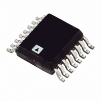
ADG3257BRQ-REEL Analog Devices Inc, ADG3257BRQ-REEL Datasheet - Page 10

ADG3257BRQ-REEL
Manufacturer Part Number
ADG3257BRQ-REEL
Description
IC MUX QUAD 3.3/5V HS 16-QSOP
Manufacturer
Analog Devices Inc
Type
Multiplexer/Demultiplexerr
Datasheet
1.ADG3257BRQZ-REEL.pdf
(12 pages)
Specifications of ADG3257BRQ-REEL
Rohs Status
RoHS non-compliant
Circuit
4 x 1:2
Independent Circuits
1
Voltage Supply Source
Single Supply
Voltage - Supply
3.3V, 5V
Operating Temperature
-40°C ~ 85°C
Mounting Type
Surface Mount
Package / Case
16-QSOP
Number Of Bits
8
Number Of Elements
1
Technology
CMOS
On Resistance
4Ohm
Propagation Delay Time
9ns
Package Type
QSOP
Operating Temp Range
-40C to 85C
Operating Temperature Classification
Industrial
Operating Supply Voltage (min)
3V
Operating Supply Voltage (typ)
3.3/5V
Operating Supply Voltage (max)
5.5V
Quiescent Current
1uA
Pin Count
16
Mounting
Surface Mount
Current - Output High, Low
-
Lead Free Status / Rohs Status
Not Compliant
ADG3257
APPLICATIONS INFORMATION
MIXED VOLTAGE OPERATION, LEVEL TRANSLATION
Bus switches can be used to provide a solution for mixed voltage
systems where interfacing bidirectionally between 5 V and 3.3 V
devices is required. To interface between 5 V and 3.3 V buses,
an external diode is placed in series with the 5 V power supply
as shown in Figure 15.
The diode drops the internal gate voltage down to 4.3 V. The
bus switch limits the voltage present on the output to
Therefore, assuming a diode drop of 0.7 V and a V
output voltage is limited to 3.3 V with a logic high.
V
CC
MICROPROCESSOR/
Figure 15. Level Translation Between 5 V and 3.3 V Devices
− External Diode Drop = V
3.3V CPU/DSP/
MEMORY
Figure 16. Input Voltage to Output Voltage
3.3V
V
0V
OUT
3.3V
BE
SWITCH
INPUT
V
CC
5V
3.3V
5V SUPPLY
= 5V
TH
5V
3.3V
V
IN
5V MEMORY
5V I/O
TH
of 1 V, the
Rev. E | Page 10 of 12
Similarly, the device could be used to translate bidirectionally
between 3.3 V to 2.5 V systems. In this case, there is no need for
an external diode. The internal V
V
3.3V
2.5V
MEMORY SWITCHING
This quad bus switch may be used to allow switching between
different memory banks, thus allowing additional memory and
decreasing capacitive loading. Figure 18 illustrates the
ADG3257 in such an application.
Figure 18. Allows Additional Memory Modules Without Added Drive or Delay
CC
Figure 17. 3.3 V to 2.5 V Level Translation Using the ADG3257 Bus Switch
= 3.3 V the bus switch limits the output voltage to
V
SDRAM NO. 1
SDRAM NO. 2
SDRAM NO. 7
SDRAM NO. 8
CC
− 1 V = 2.3 V
ADG3257
3.3V
2.5V
2.5V
BE
LOGIC
TH
2.5V
drop is 1 V, so with a
V
0V
OUT
S
SWITCH
INPUT
3.3V SUPPLY
3.3V
V
IN


