IDTQS3125S1G IDT, Integrated Device Technology Inc, IDTQS3125S1G Datasheet - Page 2
IDTQS3125S1G
Manufacturer Part Number
IDTQS3125S1G
Description
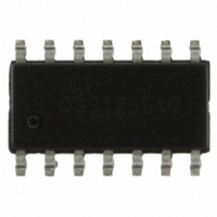
IC BUS SWITCH QUAD CMOS 14-SOIC
Manufacturer
IDT, Integrated Device Technology Inc
Series
3200r
Type
Bus Switchr
Specifications of IDTQS3125S1G
Circuit
1 x 4:1
Independent Circuits
1
Voltage Supply Source
Single Supply
Voltage - Supply
2.3 V ~ 3.6 V
Operating Temperature
-40°C ~ 85°C
Mounting Type
Surface Mount
Package / Case
14-SOIC
Number Of Bits
4
Number Of Elements
4
Technology
CMOS
High Level Output Current
-120mA
Low Level Output Current
120mA
On Resistance
10Ohm
Propagation Delay Time
6.5ns
Package Type
SOIC
Operating Temp Range
-40C to 85C
Operating Temperature Classification
Industrial
Operating Supply Voltage (min)
4.75V
Operating Supply Voltage (typ)
5V
Operating Supply Voltage (max)
5.25V
Quiescent Current
3uA
Pin Count
14
Mounting
Surface Mount
Lead Free Status / RoHS Status
Lead free / RoHS Compliant
Current - Output High, Low
-
Lead Free Status / RoHS Status
Compliant, Lead free / RoHS Compliant
Other names
800-1712
800-1712-5
800-1712
QS3125S1G
800-1712-5
800-1712
QS3125S1G


PIN CONFIGURATION
IDTQS3125
HIGH-SPEED CMOS QUADRUPLE BUS SWITCH WITH INDIVIDUAL ENABLES
GND
1OE
2OE
GND
2OE
1OE
NC
2
1
1
2
2
1
1
2
A
A
Y
Y
A
A
Y
Y
1
2
3
4
5
6
7
8
1
2
3
4
5
6
7
TOP VIEW
TOP VIEW
QSOP
SOIC
1 4
1 3
1 2
1 1
1 0
9
1 6
1 5
1 4
1 3
1 2
1 1
1 0
9
8
V
4OE
4
4
3OE
3
3
V
4OE
4
4
3OE
3
3
NC
A
Y
A
Y
CC
A
Y
A
Y
CC
2
NOTE:
1. H = HIGH Voltage Level
PIN DESCRIPTION
FUNCTION TABLE
ABSOLUTE MAXIMUM RATINGS
CAPACITANCE
NOTE:
1. This parameter is guaranteed but not production tested.
NOTES:
1. Stresses greater than those listed under ABSOLUTE MAXIMUM RATINGS may cause
2. V
3. All terminals except V
Symbol
V
V
V
V
I
P
T
OUT
Quickswitch Channels (Switch OFF)
Pin Names
L = LOW Voltage Level
X = Don't Care
1OE - 4OE
STG
permanent damage to the device. This is a stress rating only and functional operation
of the device at these or any other conditions above those indicated in the operational
sections of this specification is not implied. Exposure to absolute maximum rating
conditions for extended periods may affect reliability.
TERM
TERM
TERM
AC
MAX
CC
1
1
A
Y
xOE
terminals.
- 4
- 4
H
(2)
(3)
(3)
L
L
A
Y
Supply Voltage to Ground
DC Switch Voltage V
DC Input Voltage V
AC Input Voltage (pulse width ≤20ns)
DC Output Current
Maximum Power Dissipation (T
Storage Temperature
OE (Inputs)
Pins
xA
H
X
L
CC
I/O
I/O
I/O
Description
I
.
IN
(T
S
INDUSTRIAL TEMPERATURE RANGE
A
= +25°C, f = 1MHz, V
(1)
xY
H
X
L
Bus A
Bus Y
Bus Switch Enable
A
= 85°C)
Typ.
3
5
Description
Connect
Connect
Disconnect
–65 to +150
Max.
–0.5 to +7
–0.5 to +7
–0.5 to +7
Function
IN
5
7
Max
= 0V, V
120
0.5
–3
(1)
(1)
OUT
Unit
pF
pF
Unit
= 0V)
mA
°C
W
V
V
V
V
Related parts for IDTQS3125S1G
Image
Part Number
Description
Manufacturer
Datasheet
Request
R

Part Number:
Description:
TRANSLATION DEVICE DPI 80-PQFP
Manufacturer:
IDT, Integrated Device Technology Inc
Datasheet:
Part Number:
Description:
IDT PART
Manufacturer:
IDT, Integrated Device Technology Inc
Datasheet:
Part Number:
Description:
IC LIU T1/E1/J1 OCTAL 256PBGA
Manufacturer:
IDT, Integrated Device Technology Inc
Datasheet:

Part Number:
Description:
IC FREQ TIMING GENERATOR 28TSSOP
Manufacturer:
IDT, Integrated Device Technology Inc
Datasheet:
Part Number:
Description:
IC CLK DVR PLL 1:10 40VFQFPN
Manufacturer:
IDT, Integrated Device Technology Inc
Datasheet:
Part Number:
Description:
IC CLK FANOUT BUFFER 1:18 32LQFP
Manufacturer:
IDT, Integrated Device Technology Inc
Datasheet:
Part Number:
Description:
IC CLK FANOUT BUFFER 1:18 32LQFP
Manufacturer:
IDT, Integrated Device Technology Inc
Datasheet:
Part Number:
Description:
IC CK505 VREG/RES 56TSSOP
Manufacturer:
IDT, Integrated Device Technology Inc
Datasheet:

Part Number:
Description:
IC SDRAM CLK DVR 1:10 48-TSSOP
Manufacturer:
IDT, Integrated Device Technology Inc
Datasheet:

Part Number:
Description:
IC CLK DVR PLL 1:10 48TSSOP
Manufacturer:
IDT, Integrated Device Technology Inc
Datasheet:
Part Number:
Description:
IC FLEXPC CLK PROGR P4 56-TSSOP
Manufacturer:
IDT, Integrated Device Technology Inc
Datasheet:
Part Number:
Description:
IC FLEXPC CLK PROGR P4 56-TSSOP
Manufacturer:
IDT, Integrated Device Technology Inc
Datasheet:
Part Number:
Description:
IC FLEXPC CLK PROGR P4 56-SSOP
Manufacturer:
IDT, Integrated Device Technology Inc
Datasheet:

Part Number:
Description:
IC PLL CLK DRIVER 2.5V 28-TSSOP
Manufacturer:
IDT, Integrated Device Technology Inc
Datasheet:
Part Number:
Description:
IC CLOCK DRIVER 2.5V 24-TSSOP
Manufacturer:
IDT, Integrated Device Technology Inc
Datasheet: