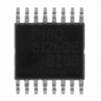
PI3C3125QEX Pericom Semiconductor, PI3C3125QEX Datasheet - Page 3

PI3C3125QEX
Manufacturer Part Number
PI3C3125QEX
Description
IC 4-BIT BUS SW 2-PORT 16-QSOP
Manufacturer
Pericom Semiconductor
Type
FET Bus Switchr
Datasheet
1.PI3C3126QE.pdf
(7 pages)
Specifications of PI3C3125QEX
Circuit
4 x 1:1
Voltage Supply Source
Single Supply
Voltage - Supply
3 V ~ 3.6 V
Mounting Type
Surface Mount
Package / Case
16-QSOP
Number Of Bits
4
Number Of Elements
4
Technology
CMOS
High Level Output Current
-120mA
Low Level Output Current
120mA
On Resistance
8(Typ)Ohm
Propagation Delay Time
9.8ns
Package Type
QSOP
Operating Temp Range
-40C to 85C
Operating Temperature Classification
Industrial
Operating Supply Voltage (typ)
2.5/3.3V
Operating Supply Voltage (max)
3.63V
Quiescent Current
500uA
Pin Count
16
Mounting
Surface Mount
Lead Free Status / RoHS Status
Lead free / RoHS Compliant
Operating Temperature
-
Current - Output High, Low
-
Independent Circuits
-
Lead Free Status / Rohs Status
Compliant
DC Electrical Characteristics
Notes:
1. For Max. or Min. conditions, use appropriate value specifi ed under Electrical Characteristics for the applicable device type.
2. Typical values are at V
3. Not more than one output should be shorted at one time. Duration of the test should not exceed one second.
4. Measured by the voltage drop between A and B pin at indicated current through the switch. ON resistance is determined by the
Capacitance
Notes:
1. This parameter is determined by device characterization but is not production tested.
Power Supply Characteristics
Notes:
1. For Max. or Min. conditions, use appropriate value specifi ed under Electrical Characteristics for the applicable device.
2. Typical values are at V CC = 3.3V, +25°C ambient.
3. Per driven input (control input only); A and B pins do not contribute to ΔI CC .
Parameters
V
V
I
I
I
V
R
Parameters
C
C
C
Parameters
I
∆I
IH
IL
OZH
CC
ON
IN
OFF
ON
IH
IL
IK
lower of the voltages on the two (A,B) pins.
CC
(3)
09-0075
(1)
(T
Description
Input HIGH Voltage
Input LOW Voltage
Input HIGH current
Input LOW Current
High Impedance Output
Current
Clamp Diode Voltage
Switch ON Resistance
A
Description
Quiescent Power
Supply Current
Supply Current per
Input HIGH
Description
Input Capacitance
A/B Capacitance, Switch Off
A/B Capacitance, Switch On
= 25°C, f = 1 MHz)
CC
= 3.3V, T
A
(Over Operating Range, T
= 25°C ambient and maximum loading.
(4)
Test Conditions
V
V
CC
CC
Test Conditions(1)
Guearanteed Logic HIGH Level
Guaranteed Logic LOW Level –0.5
V
V
V
V
V
CC
CC
CC
CC
CC
= Max
= Max
0 ≤ A, B ≤ V
= Min., I
= Min., V
= Max., V
= Max., V
= Min., V
IN
IN
IN
IN
IN
CC
= –18mA
V
V
= 2.4V, I
= 0.0V, I
Test Conditions
= V
= GND
IN
IN
A
3
V IN = 0V
V IN = 0V
V IN = 0V
= –40°C to +85°C, V
= GND or V
= 3.0V
CC
2.5V/3.3V, High Bandwidth, Hot Insertion,4-Bit,
ON
ON
(3)
= 15mA
= 48mA or 60mA
2-Port Bus Switch with Individual Enables
CC
CC
Min.
Typ.
3.5
5.0
10.0
= 3.3V ±10%)
Min.
2.0
Typ.
260
Units
pF
Typ.(2)
0.8
–0.73
5
8
(2)
Max.
500
750
PS8344
Max
±1
±1
±1
–1.2
7
15
PI3C3125
Units
μA
Units
V
μA
V
-Ohm
11/04/09


