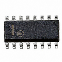
MC74HC138ADR2G ON Semiconductor, MC74HC138ADR2G Datasheet - Page 5

MC74HC138ADR2G
Manufacturer Part Number
MC74HC138ADR2G
Description
IC DECODER/DEMUX 1-8 HP 16SOIC
Manufacturer
ON Semiconductor
Series
74HCr
Type
Decoder/Demultiplexerr
Datasheet
1.MC74HC138ANG.pdf
(9 pages)
Specifications of MC74HC138ADR2G
Circuit
1 x 3:8
Independent Circuits
1
Current - Output High, Low
5.2mA, 5.2mA
Voltage Supply Source
Single Supply
Voltage - Supply
2 V ~ 6 V
Operating Temperature
-55°C ~ 125°C
Mounting Type
Surface Mount
Package / Case
16-SOIC (3.9mm Width)
Product
Decoders, Encoders, Multiplexers & Demultiplexers
Logic Family
74HC
Number Of Bits
3
Number Of Lines (input / Output)
1.0 / 8.0
Supply Voltage (max)
6 V
Supply Voltage (min)
2 V
Maximum Operating Temperature
+ 125 C
Minimum Operating Temperature
- 55 C
Mounting Style
SMD/SMT
Number Of Input Lines
1.0
Number Of Output Lines
8.0
Logic Type
Decoder / Demultiplexer
No. Of Outputs
8
Supply Voltage Range
2V To 6V
Logic Case Style
SOIC
No. Of Pins
16
Operating Temperature Range
-55°C To +125°C
Filter Terminals
SMD
Rohs Compliant
Yes
Family Type
HC
Lead Free Status / RoHS Status
Lead free / RoHS Compliant
Other names
MC74HC138ADR2GOS
MC74HC138ADR2GOS
MC74HC138ADR2GOSTR
MC74HC138ADR2GOS
MC74HC138ADR2GOSTR
Available stocks
Company
Part Number
Manufacturer
Quantity
Price
Company:
Part Number:
MC74HC138ADR2G
Manufacturer:
ON
Quantity:
887
Company:
Part Number:
MC74HC138ADR2G
Manufacturer:
ON Semiconductor
Quantity:
37 386
Company:
Part Number:
MC74HC138ADR2G
Manufacturer:
ON Semiconductor
Quantity:
8 300
Part Number:
MC74HC138ADR2G
Manufacturer:
ON/安森美
Quantity:
20 000
ADDRESS INPUTS
A0, A1, A2 (Pins 1, 2, 3)
determine which of the eight outputs is active−low.
CONTROL INPUTS
CS1, CS2, CS3 (Pins 6, 4, 5)
at a low level, the chip is selected and the outputs follow the
Address inputs. These inputs, when the chip is selected,
Chip select inputs. For CS1 at a high level and CS2, CS3
OUTPUT Y
OUTPUT Y
CS2, CS3
INPUT A
INPUT
t
PLH
90%
50%
10%
50%
50%
VALID
90%
50%
t
10%
f
Figure 1.
Figure 3.
t
PHL
t
THL
VALID
t
PHL
t
r
t
PLH
SWITCHING WAVEFORMS
t
TLH
PIN DESCRIPTIONS
http://onsemi.com
V
GND
V
GND
CC
CC
5
INPUT CS1
Address inputs. For any other combination of CS1, CS2, and
CS3, the outputs are at a logic high.
OUTPUTS
Y0 − Y7 (Pins 15, 14, 13, 12, 11, 10, 9, 7)
low level when addressed and the chip is selected. These
outputs remain high when not addressed or the chip is not
selected.
OUTPUT Y
Active−low Decoded outputs. These outputs assume a
t
PHL
*Includes all probe and jig capacitance
t
THL
10%
DEVICE
UNDER
Figure 4. Test Circuit
50%
TEST
90%
90%
50%
t
10%
r
Figure 2.
OUTPUT
TEST POINT
t
f
C
L
t
PLH
*
t
TLH
V
GND
CC


