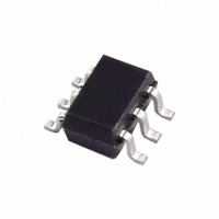
ADG3241BKS-500RL7 Analog Devices Inc, ADG3241BKS-500RL7 Datasheet - Page 3

ADG3241BKS-500RL7
Manufacturer Part Number
ADG3241BKS-500RL7
Description
IC SW BUS 2.5-3.3V 1BIT SC70-6
Manufacturer
Analog Devices Inc
Type
Bus Switchr
Datasheet
1.ADG3241BKSZ-REEL.pdf
(16 pages)
Specifications of ADG3241BKS-500RL7
Circuit
1 x 1:1
Independent Circuits
1
Voltage Supply Source
Single Supply
Voltage - Supply
2.5V, 3.3V
Operating Temperature
-40°C ~ 85°C
Mounting Type
Surface Mount
Package / Case
SC-70-6, SC-88, SOT-363
Lead Free Status / RoHS Status
Contains lead / RoHS non-compliant
Current - Output High, Low
-
SPECIFICATIONS
V
Table 1.
Parameter
DC ELECTRICAL CHARACTERISTICS
CAPACITANCE
SWITCHING CHARACTERISTICS
DIGITAL SWITCH
POWER REQUIREMENTS
1
2
3
4
5
6
Temperature range is as follows: B Version: −40°C to +85°C.
Typical values are at 25°C, unless otherwise stated.
Guaranteed by design, not subject to production test.
The digital switch contributes no propagation delay other than the RC delay of the typical R
source. Since the time constant is much smaller than the rise/fall times of typical driving signals, it adds very little propagation delay to the system. Propagation delay
of the digital switch, when used in a system, is determined by the driving circuit on the driving side of the switch and its interaction with the load on the driven side.
See Timing Measurement Information section.
This current applies to the Control Pin BE only. The A and B ports contribute no significant ac or dc currents as they transition.
CC
Input High Voltage
Input Low Voltage
Input Leakage Current
Off State Leakage Current
On State Leakage Current
Maximum Pass Voltage
A Port Off Capacitance
B Port Off Capacitance
A, B Port On Capacitance
Control Input Capacitance
Propagation Delay A to B or B to A, t
Bus Enable Time BE to A or B
Bus Disable Time BE to A or B
Bus Enable Time BE to A or B
Bus Disable Time BE to A or B
Bus Enable Time BE to A or B
Bus Disable Time BE to A or B
Maximum Data Rate
Channel Jitter
On Resistance
V
Quiescent Power Supply Current
Increase in I
CC
= 2.3 V to 3.6 V, GND = 0 V, all specifications T
3
CC
per Input
6
3
5
5
5
5
5
5
PD
4
Symbol
V
V
V
V
I
I
V
C
C
C
C
t
t
t
t
t
t
t
R
I
∆I
I
OZ
CC
PHL
PZH
PHZ
PZH
PHZ
PZH
PHZ
INH
INH
INL
INL
P
ON
A
B
A
IN
CC
, C
OFF
OFF
, t
, t
, t
, t
, t
, t
, t
B
PLH
PZL
PLZ
PZL
PLZ
PZL
PLZ
ON
MIN
to T
Conditions
V
V
V
V
0 ≤ A, B ≤ V
0 ≤ A, B ≤ V
V
V
V
f = 1 MHz
f = 1 MHz
f = 1 MHz
f = 1 MHz
C
V
V
V
V
V
V
V
V
V
V
V
V
V
V
Digital Inputs = 0 V or V
Digital Inputs = 0 V or V
V
CC
CC
CC
CC
A
A
A
L
CC
CC
CC
CC
CC
CC
CC
CC
CC
CC
CC
CC
CC
CC
CC
/V
/V
/V
MAX
= 50 pF, V
= 2.7 V to 3.6 V
= 2.3 V to 2.7 V
= 2.7 V to 3.6 V
= 2.3 V to 2.7 V
= 3.0 V to 3.6 V; SEL = V
= 3.0 V to 3.6 V; SEL = V
= 3.0 V to 3.6 V; SEL = 0 V
= 3.0 V to 3.6 V; SEL = 0 V
= 2.3 V to 2.7 V; SEL = V
= 2.3 V to 2.7 V; SEL = V
= SEL = 3.3 V; V
= SEL = 3.3 V; V
= 3 V, SEL = V
= 3 V, SEL = V
= 2.3 V, SEL = V
= 2.3 V, SEL = V
= 3 V, SEL = 0 V, V
= 3 V, SEL = 0 V, V
= 3.6 V, BE = 3.0 V; SEL = V
Rev. B | Page 3 of 16
B
B
B
= V
= V
= V
, unless otherwise noted.
CC
CC
CC
= SEL = 3.3 V, I
= SEL = 2.5 V, I
= 3.3 V, SEL = 0 V, I
CC
CC
CC
= SEL = 3 V
CC
CC
, V
, V
A
A
CC
CC
/V
/V
ON
, V
, V
A
A
A
A
of the switch and the load capacitance when driven by an ideal voltage
B
B
= 0 V, I
= 1.7 V, I
= 0 V, I
= 1 V, I
A
A
= 2 V
= 2 V
CC
CC
= 0 V, I
= 1 V, I
; SEL = V
; SEL = 0 V
O
O
CC
CC
CC
CC
= −5 μA
= −5 μA
BA
BA
BA
CC
O
BA
BA
BA
= 8 mA
= 8 mA
= −5 μA
= 8 mA
1
= 8 mA
= 8 mA
= 8 mA
CC
Min
2.0
1.7
2.2
1.5
1.5
1
1
1
1
1
1
2.3
B Version
Typ
±0.01
±0.01
±0.01
2.5
1.8
1.8
3.5
3.5
7
4
3.2
3
3
2.5
3
2.5
1.5
45
4.5
12
5
9
5
12
0.01
0.1
0.15
2
Max
0.8
0.7
±1
±1
±1
2.7
2.1
2.1
0.225
4.6
4
4
3.8
4
3.4
8
28
9
18
8
3.6
1
0.2
8
ADG3241
Unit
V
V
V
V
μA
μA
μA
V
V
V
pF
pF
pF
pF
ns
ns
ns
ns
ns
ns
ns
Gbps
ps p-p
Ω
Ω
Ω
Ω
Ω
Ω
V
μA
mA
μA


