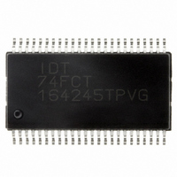
IDT74FCT164245TPVG8 IDT, Integrated Device Technology Inc, IDT74FCT164245TPVG8 Datasheet - Page 5

IDT74FCT164245TPVG8
Manufacturer Part Number
IDT74FCT164245TPVG8
Description
XLATOR 16BIT BIDIR CMOS 48-SSOP
Manufacturer
IDT, Integrated Device Technology Inc
Series
74FCTr
Datasheet
1.IDT74FCT164245TPVG8.pdf
(8 pages)
Specifications of IDT74FCT164245TPVG8
Logic Function
Translator, Bidirectional, 3-State
Number Of Bits
8
Input Type
Voltage
Output Type
Voltage
Number Of Channels
2
Number Of Outputs/channel
8
Differential - Input:output
No/No
Propagation Delay (max)
5ns
Voltage - Supply
2.7 V ~ 3.6 V
Operating Temperature
-40°C ~ 85°C
Package / Case
48-SSOP
Supply Voltage
2.7 V ~ 5.5 V
Lead Free Status / RoHS Status
Lead free / RoHS Compliant
Data Rate
-
Other names
74FCT164245TPVG8
800-1606-2
800-1606-2
Available stocks
Company
Part Number
Manufacturer
Quantity
Price
Company:
Part Number:
IDT74FCT164245TPVG8
Manufacturer:
PMC
Quantity:
129
NOTES:
1. For conditions shown as Min. or Max., use appropriate value specified under Electrical Characteristics for the applicable device type.
2. Typical values are at V
3. Per TTL driven input. All other inputs at V
4. This parameter is not directly testable, but is derived for use in Total Power Supply Calculations.
5. Values for these conditions are examples of the I
6. I
POWER SUPPLY CHARACTERISTICS
IDT74FCT164245T
FAST CMOS 16-BIT BIDIRECTIONAL 3.3V TO 5V TRANSLATOR
Symbol
I
I
I
ΔI
D
N
I
f
N
fi = Input Frequency
Ni = Number of Inputs at fi
C
C
CC1
CC2
CCD
CP
H
T
CP
ΔI
I
CC
= I
= I
CCD
I
= Number of TTL Inputs at D
= Duty Cycle for TTL Inputs High
C
= Clock Frequency for Register Devices (Zero for Non-Register Devices)
CC
= Number of Clock Inputs at f
QUIESCENT
= Quiescent Current (I
= Quiescent Current (I
= Dynamic Current caused by an Input Transition Pair (HLH or LHL)
CC1
= Power Supply Current for a TTL High Input
+ I
CC2
Quiescent Power Supply Current
TTL Inputs HIGH
Dynamic Power Supply
Current
Total Power Supply Current
+ I
+ ΔI
INPUTS
CC
(4)
CC1
D
+ I
H
N
DYNAMIC
CC1L
CC2L
Parameter
= 5V, V
T
+ I
, I
, I
CCD
H
CC1H
CC2H
CP
CC2
(f
CP
and I
and I
= 3.3V, +25°C ambient.
N
CP
CC
(6)
CC1Z
CC2Z
/2 + fiNi)
or GND.
)
)
CC
formula. These limits are guaranteed but not tested.
V
V
V
Outputs Open
xOE = xDIR = GND
One Input Togging
50% Duty Cycle
V
Outputs Open
f
50% Duty Cycle
xOE = xDIR = GND
One Bit Toggling
V
Outputs Open
f
50% Duty Cycle
xOE = xDIR = GND
Sixteen Bits Toggling
I
I
IN
CC1
CC1
CC1
CC1
= 10MHz
= 2.5MHz
= V
= Max., V
= Max., V
= Max., V
= Max., V
CC2
- 0.6V
CC2
CC2
CC2
CC2
(3)
Test Conditions
= Max.
= Max.
= Max.
= Max.
5
V
V
V
V
V
V
(1)
IN
IN
IN
IN
IN
IN
= V
= V
= V
= GND
= GND
= GND
CC2
CC2
CC2
- 0.6V
- 0.6V
INDUSTRIAL TEMPERATURE RANGE
Min.
—
—
—
—
Typ.
1.2
3.5
12
75
(2)
Max.
8.5
120
4.7
30
(5)
MHz
Unit
µA/
mA
µ A


