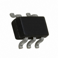
FXLP34P5X Fairchild Semiconductor, FXLP34P5X Datasheet - Page 8

FXLP34P5X
Manufacturer Part Number
FXLP34P5X
Description
TRANSLATOR 1BIT UNIDIRECT SC70-5
Manufacturer
Fairchild Semiconductor
Datasheet
1.FXLP34L6X.pdf
(12 pages)
Specifications of FXLP34P5X
Logic Function
Translator, Unidirectional
Number Of Bits
1
Input Type
Voltage
Output Type
Voltage
Number Of Channels
1
Number Of Outputs/channel
1
Differential - Input:output
No/No
Propagation Delay (max)
3ns
Voltage - Supply
1 V ~ 3.6 V
Operating Temperature
-40°C ~ 85°C
Package / Case
SC-70-5, SC-88A, SOT-323-5, SOT-353, 5-TSSOP
Supply Voltage
1 V ~ 3.6 V
Logic Family
FXLP
Logic Type
Voltage Level Translation
Number Of Channels Per Chip
Single
Polarity
Non-Inverting
Supply Voltage (max)
3.6 V
Supply Voltage (min)
1 V
Maximum Operating Temperature
+ 85 C
Mounting Style
SMD/SMT
High Level Output Current
- 2.6 mA
Input Bias Current (max)
0.9 uA
Low Level Output Current
2.6 mA
Minimum Operating Temperature
- 40 C
Propagation Delay Time
48.6 ns @ 1 V
Number Of Lines (input / Output)
1 / 1
Lead Free Status / RoHS Status
Lead free / RoHS Compliant
Data Rate
-
Lead Free Status / Rohs Status
Lead free / RoHS Compliant
Other names
FXLP34P5XTR
FXLP34P5X_NL
FXLP34P5X_NLTR
FXLP34P5X_NLTR
FXLP34P5X_NL
FXLP34P5X_NLTR
FXLP34P5X_NLTR
Available stocks
Company
Part Number
Manufacturer
Quantity
Price
Company:
Part Number:
FXLP34P5X
Manufacturer:
EXAR
Quantity:
14 300
Company:
Part Number:
FXLP34P5X
Manufacturer:
Fairchild Semiconductor
Quantity:
93 797
Part Number:
FXLP34P5X
Manufacturer:
FAIRCHILD/ن»™ç«¥
Quantity:
20 000
© 2006 Fairchild Semiconductor Corporation
FXLP34 • Rev. 1.0.4
Translator Power-up Sequence Recommendations
To ensure that the system does not experience
unnecessary I
oscillations during power-up; adhere to the following
guidelines. This device is designed with the output pin(s)
supplied by V
The first recommendation is to begin by powering up the
input side of the device with V
should be ramped with or ahead of V
This guards against bus contentions and oscillations as
AC Loadings and Waveforms
Table 1.
Symbol
V
V
mo
mi
AC Load Table
3.3V ±0.3V
CC
CC
1.5V
1.5V
and the input pin(s) supplied by V
current draw, bus contention, or
Figure 4. Waveform for Inverting and Non-Inverting Functions
2.5V ±0.2V
CC1
V
V
CC1
CC
. The Input pin(s)
/2
CC1
/2
or held LOW.
Figure 3. AC Test Circuit
1.8V ±0.15V
V
CC1
V
CC1
CC
.
/2
/2
8
all inputs and the input V
time. The output V
voltage level to which the device will translate. The
output pin(s) then translate to logic levels dictated by the
output V
Upon completion of these steps, the device can be
configured for the desired operation. Following these
steps helps prevent possible damage to the translator
device as well as other system components.
V
CC
1.5V ±0.10V
CC
V
V
CC1
levels.
CC
/2
/2
CC
can then be powered to the target
1.2V ±0.10V
CC1
V
V
CC1
C
are powered at the same
C/2
/2
www.fairchildsemi.com
V
V
1.0V
CC1
CC
/2
/2


