MAX3394EEBL+T Maxim Integrated Products, MAX3394EEBL+T Datasheet - Page 12
MAX3394EEBL+T
Manufacturer Part Number
MAX3394EEBL+T
Description
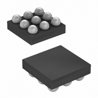
IC LVL XLTR LV 6MBPS PP 9-UCSP
Manufacturer
Maxim Integrated Products
Datasheet
1.MAX3394EEBLT.pdf
(20 pages)
Specifications of MAX3394EEBL+T
Logic Function
Translator, Bidirectional, 3-State
Number Of Bits
2
Input Type
Logic
Output Type
Logic
Data Rate
6Mbps
Number Of Channels
2
Number Of Outputs/channel
1
Differential - Input:output
No/No
Propagation Delay (max)
50ns
Voltage - Supply
1.65 V ~ 5.5 V
Operating Temperature
-40°C ~ 85°C
Package / Case
9-UCSP®
Supply Voltage
1.65 V ~ 5.5 V
Lead Free Status / RoHS Status
Lead free / RoHS Compliant
Other names
MAX3394EEBL+T
MAX3394EEBL+TTR
MAX3394EEBL+TTR


itance with a characteristic RC charging waveform.
When the low-to-high transition threshold (V
TH
sourcing 15mA to fully charge the bus capacitance.
External pullup resistors reduce the time needed to
reach the low-to-high transition threshold, thereby
increasing the data rate. In the logic-low state however,
external pullup resistors increase the DC current
through the internal pass-FET, increasing the output
voltage of the device.
The MAX3395E provides level translation for Class A, B,
and C smart cards. When supply voltage V
rupted due to the disconnection of a smart card, the
device does not latch up. Normal operation resumes
±15kV ESD-Protected, High-Drive Current, Dual-/Quad-/
Octal-Level Translators with Speed-Up Circuitry
12
) is reached, the rise time accelerators switch on,
______________________________________________________________________________________
+1.8V
CONTROLLER
Smart-Card Interface
SYSTEM
+1.8V
I/O V
GND
L_
DATA
CLK
EN
V
L
M
M
P1
N3
V
CC-TH
L
0.1μF
CC
is inter-
EN
I/O V
I/O V
or V
V
L
L
L
MAX3394E
GATE CONTROL
ENHANCEMENT
1
2
L-
N-CHANNEL
SLEW-RATE
PASS-FET
GND
I/O V
V
I/O V
CC
CC
CC
upon restoration of the V
MAX3395E provides bidirectional level translation on
four I/O lines, making it well suited for buffering and
translating 4-wire serial interfaces.
For the latest application details on UCSP construction,
dimensions, tape carrier information, PCB techniques,
bump-pad layout, and recommended reflow temperature
profiles, as well as the latest information on reliability test-
ing results, go to Maxim’s web site at
ic.com/ucsp
Wafer-Level Packaging (WLP) and Its Applications .
2
1
UCSP Applications Information
0.1μF
V
CC
M
M
P2
N4
Typical Operating Circuit
1μF
to find the Application Note 1891:
V
CC
CLK
DATA
I/O V
SYSTEM
+3.3V
GND
CC_
Functional Diagram
+3.3V
CC
supply voltage. The
www.maxim-
Related parts for MAX3394EEBL+T
Image
Part Number
Description
Manufacturer
Datasheet
Request
R

Part Number:
Description:
�15kV ESD-Protected, High-Drive Current, Dual-/Quad-/ Octal-Level Translators with Speed-Up Circuitry
Manufacturer:
MAXIM [Maxim Integrated Products]
Datasheet:

Part Number:
Description:
MAX7528KCWPMaxim Integrated Products [CMOS Dual 8-Bit Buffered Multiplying DACs]
Manufacturer:
Maxim Integrated Products
Datasheet:
Part Number:
Description:
Single +5V, fully integrated, 1.25Gbps laser diode driver.
Manufacturer:
Maxim Integrated Products
Datasheet:
Part Number:
Description:
Single +5V, fully integrated, 155Mbps laser diode driver.
Manufacturer:
Maxim Integrated Products
Datasheet:
Part Number:
Description:
VRD11/VRD10, K8 Rev F 2/3/4-Phase PWM Controllers with Integrated Dual MOSFET Drivers
Manufacturer:
Maxim Integrated Products
Datasheet:
Part Number:
Description:
Highly Integrated Level 2 SMBus Battery Chargers
Manufacturer:
Maxim Integrated Products
Datasheet:
Part Number:
Description:
Current Monitor and Accumulator with Integrated Sense Resistor; ; Temperature Range: -40°C to +85°C
Manufacturer:
Maxim Integrated Products
Part Number:
Description:
TSSOP 14/A�/RS-485 Transceivers with Integrated 100O/120O Termination Resis
Manufacturer:
Maxim Integrated Products
Part Number:
Description:
TSSOP 14/A�/RS-485 Transceivers with Integrated 100O/120O Termination Resis
Manufacturer:
Maxim Integrated Products
Part Number:
Description:
QFN 16/A�/AC-DC and DC-DC Peak-Current-Mode Converters with Integrated Step
Manufacturer:
Maxim Integrated Products
Part Number:
Description:
TDFN/A/65V, 1A, 600KHZ, SYNCHRONOUS STEP-DOWN REGULATOR WITH INTEGRATED SWI
Manufacturer:
Maxim Integrated Products
Part Number:
Description:
Integrated Temperature Controller f
Manufacturer:
Maxim Integrated Products
Part Number:
Description:
SOT23-6/I�/45MHz to 650MHz, Integrated IF VCOs with Differential Output
Manufacturer:
Maxim Integrated Products
Part Number:
Description:
SOT23-6/I�/45MHz to 650MHz, Integrated IF VCOs with Differential Output
Manufacturer:
Maxim Integrated Products
Part Number:
Description:
EVALUATION KIT/2.4GHZ TO 2.5GHZ 802.11G/B RF TRANSCEIVER WITH INTEGRATED PA
Manufacturer:
Maxim Integrated Products