PI4ULS3V16AE Pericom Semiconductor, PI4ULS3V16AE Datasheet - Page 2
PI4ULS3V16AE
Manufacturer Part Number
PI4ULS3V16AE
Description
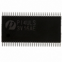
IC VOLT TRANSLATOR 56-TSSOP
Manufacturer
Pericom Semiconductor
Datasheet
1.PI4ULS3V16AEX.pdf
(10 pages)
Specifications of PI4ULS3V16AE
Logic Function
Level Shifter, Bidirectional, 3-State
Number Of Bits
16
Input Type
Voltage
Output Type
Voltage
Data Rate
180Mbps
Number Of Channels
16
Number Of Outputs/channel
1
Differential - Input:output
No/No
Propagation Delay (max)
3.5ns
Voltage - Supply
1.2 V ~ 3.6 V
Operating Temperature
-40°C ~ 85°C
Package / Case
56-TSSOP
Supply Voltage
1.2 V ~ 3.6 V
Number Of Channels Per Chip
16
High Level Output Current
- 12 mA
Low Level Output Current
12 mA
Propagation Delay Time
3.5 ns
Supply Voltage (max)
3.6 V
Supply Voltage (min)
1.2 V
Maximum Operating Temperature
+ 85 C
Function
Bus Transceiver with Voltage Translation
Input Bias Current (max)
10 uA
Minimum Operating Temperature
- 40 C
Mounting Style
SMD/SMT
Number Of Circuits
2
Polarity
Non-Inverting
Lead Free Status / RoHS Status
Lead free / RoHS Compliant


Maximum Ratings
(Absolute maximum ratings over operating free-air temperature range, unless otherwise noted)
Note:
1.
2.
3.
4.
Pin Confi guration - TSSOP
Supply voltage range:
Input voltage range, V
Voltage Range applied to any I/O pins in the high-impedance
or Power-Off state, V
Voltage Range applied to any I/O pins in the High or Low
state V
The input negative voltage and output voltage ratings may be exceeded if the input and output current ratings are observed.
This value is limited to 3.6V maximum.
The package thermal impedance is calculated in accordance with JESD 51.
Stresses greater than those listed under MAXIMUM RAT INGS may cause permanent damage to the device. This is a stress rating only and
functional operation of the device at these or any other conditions above those in di cat ed in the operational sec tions of this spec i fi ca tion is not
im plied. Exposure to absolute maximum rating conditions for ex tend ed periods may affect reliability.
11-0008
IO
(1, 2)
TEST_EN
:
TST
1
V
V
V
V
2
GND
GND
GND
GND
SEL
SEL
CCB
CCB
CCB
CCB
1
1
1
1
1
1
1
1
2
2
2
2
2
2
2
2
B
B
B
B
B
B
B
B
B
B
B
B
B
B
B
B
B
1
2
3
4
5
6
7
8
1
2
3
4
5
6
7
8
IO
I
(1)
(1)
1
2
3
4
5
6
7
8
9
10
11
12
13
14
15
16
17
18
19
20
21
22
23
24
25
26
27
28
:
V
V
Control Inputs ...... –0.5V to 4.6V
A Port
B Port ................... –0.5V to 4.6V
A Port
B Port ....... –0.5V to V
CCA
CCB
.................... –0.5V to 4.6V
.................... –0.5V to 4.6V
56
55
54
53
52
51
50
49
48
47
46
45
44
43
42
41
40
39
38
37
36
35
34
33
32
31
30
29
.........
.......................
–0.5V to V
OUT_SEL
1
V
1
1
GND
1
1
V
1
1
GND
1
1
2
2
GND
2
2
V
2
2
GND
2
2
V
2
TST
OE
A
A
A
A
A
A
A
A
A
A
A
A
A
A
A
A
OE
CCA
CCA
CCA
CCA
1
2
3
4
5
6
7
8
1
2
3
4
5
6
7
8
A
–0.5V to 4.6V
CCA
CCB
+0.5V
+0.5V
2
Pin Confi guration - TQFN
Input clamp current, I
Output clamp current, I
Continuous output current, I
Continuous current through V
Package thermal impedance, 0
Storage temperature range, T
Level Shifter with Automatic Direction Control
V
V
GND
GND
GND
GND
CCB
CCB
1
1
1
1
1
1
1
2
2
2
2
2
2
2
B
B
B
B
B
B
B
B
B
B
B
B
B
B
2
3
4
5
6
7
8
1
2
3
4
5
6
7
1.2V to 3.6V, Universal Bi-directional
10
11
12
13
14
15
16
17
18
19
20
1
2
3
4
5
6
7
8
9
IK
OK
(V
A package ............................. 82°C/W
ZF package ........................... 33°C/W
(V
I
<0) ................................... –50mA
O
STG
O
CCA,
....................................... ±20mA
JA
<0) .............................. –50mA
(3)
.................... –65°C to 150°C
V
:
CCB
or GND ..... ±100mA
48
47
46
45
44
43
42
41
40
39
38
37
36
35
34
33
32
31
30
29
PI4ULS3V16
PS8775F
1
GND
1
1
V
1
1
GND
1
1
2
2
GND
2
2
V
2
2
GND
2
A
A
A
A
A
A
A
A
A
A
A
A
A
A
CCA
CCA
2
3
4
5
6
7
8
1
2
3
4
5
6
7
07/21/08
Related parts for PI4ULS3V16AE
Image
Part Number
Description
Manufacturer
Datasheet
Request
R

Part Number:
Description:
Fast CMOS bus interface register
Manufacturer:
Pericom Semiconductor
Datasheet:
Part Number:
Description:
4-bit,4-port bus exchange switch
Manufacturer:
Pericom Semiconductor
Datasheet:
Part Number:
Description:
Manufacturer:
Pericom Semiconductor
Datasheet:
Part Number:
Description:
Manufacturer:
Pericom Semiconductor
Datasheet:
Part Number:
Description:
Manufacturer:
Pericom Semiconductor
Datasheet:
Part Number:
Description:
Manufacturer:
Pericom Semiconductor
Datasheet:
Part Number:
Description:
Manufacturer:
Pericom Semiconductor
Datasheet:
Part Number:
Description:
Manufacturer:
Pericom Semiconductor
Datasheet:
Part Number:
Description:
Manufacturer:
Pericom Semiconductor
Datasheet:
Part Number:
Description:
Manufacturer:
Pericom Semiconductor
Datasheet:
Part Number:
Description:
Manufacturer:
Pericom Semiconductor
Datasheet:
Part Number:
Description:
Manufacturer:
Pericom Semiconductor
Datasheet:
Part Number:
Description:
Manufacturer:
Pericom Semiconductor
Datasheet:
Part Number:
Description:
Manufacturer:
Pericom Semiconductor
Datasheet: