NLSV4T244MUTAG ON Semiconductor, NLSV4T244MUTAG Datasheet

IC XLATOR 4BIT DUAL 12-UQFN

NLSV4T244MUTAG

Manufacturer Part Number
NLSV4T244MUTAG
Description
IC XLATOR 4BIT DUAL 12-UQFN
Manufacturer
ON Semiconductor
Datasheet

Specifications of NLSV4T244MUTAG

Logic Function
Translator, 3-State
Number Of Bits
4
Input Type
Voltage
Output Type
Voltage
Number Of Channels
4
Number Of Outputs/channel
1
Differential - Input:output
No/No
Propagation Delay (max)
1.6ns
Voltage - Supply
0.9 V ~ 4.5 V
Operating Temperature
-40°C ~ 85°C
Package / Case
12-UFQFN
Supply Voltage
3 V ~ 3.6 V
Low Level Output Current
24mA
Abs. Propagation Delay Time
5.3ns
Mounting
Surface Mount
Pin Count
12
Operating Temperature (min)
-40C
Operating Temperature (max)
85C
Operating Temperature Classification
Industrial
High Level Output Current
-24mA
Operating Supply Voltage (typ)
1.8/2.5/3.3V
Operating Supply Voltage (max)
4.5V
Operating Supply Voltage (min)
0.9V
Lead Free Status / RoHS Status
Lead free / RoHS Compliant
Data Rate
-
Lead Free Status / Rohs Status
Compliant

Available stocks

Company
Part Number
Manufacturer
Quantity
Price
Part Number:
NLSV4T244MUTAG
0
Company:
Part Number:
NLSV4T244MUTAG
Quantity:
56
Company:
Part Number:
NLSV4T244MUTAG
Quantity:
2 500
NLSV4T244
4-Bit Dual-Supply
Non-Inverting Level
Translator
translator. The input A
different power supply rails, V
supply rails are configurable from 0.9 V to 4.5 V allowing universal
low−voltage translation from the input A
Features
Typical Applications
Important Information
© Semiconductor Components Industries, LLC, 2009
December, 2009 − Rev. 3
The NLSV4T244 is a 4−bit configurable dual−supply voltage level
Wide V
High−Speed w/ Balanced Propagation Delay
Inputs and Outputs have OVT Protection to 4.5 V
Non−preferential V
Outputs at 3−State until Active V
Power−Off Protection
Outputs Switch to 3−State with V
Ultra−Small Packaging: 1.7 mm x 2.0 mm UQFN12
These are Pb−Free Devices
Mobile Phones, PDAs, Other Portable Devices
ESD Protection for All Pins:
CCA
HBM (Human Body Model) > 1500 V
and V
CCB
CCA
n
and output B
Operating Range: 0.9 V to 4.5 V
and V
CCB
CCA
CC
CCB
n
Sequencing
ports are designed to track two
and V
is Reached
n
at GND
to the output B
CCB
respectively. Both
n
port.
1
14
†For information on tape and reel specifications,
NLSV4T244MUTAG
NLSV4T244DR2G
NLSV4T244DTR2G TSSOP14
14
including part orientation and tape sizes, please
refer to our Tape and Reel Packaging Specification
Brochure, BRD8011/D.
1
(Note: Microdot may be in either location)
1
A
L, WL
Y, YY
W, WW
G or G
(Note: Microdot may be in either location)
Device
1
ORDERING INFORMATION
UR = Specific Device Code
M
G
CASE 523AE
http://onsemi.com
CASE 751A
MU SUFFIX
= Assembly Location
= Wafer Lot
= Year
= Work Week
= Pb−Free Package
= Date Code
= Pb−Free Package
D SUFFIX
CASE 948G
SOIC−14
DT SUFFIX
TSSOP−14
UQFN12
(Pb−Free)
(Pb−Free)
(Pb−Free)
Package
UQFN12
SO−14
Publication Order Number:
14
1
3000/Tape & Reel
2500/Tape & Reel
2500/Tape & Reel
DIAGRAMS
14
MARKING
SV4T244G
AWLYWW
1
NLSV4T244/D
Shipping
URMG
ALYWG
SV4T
G
244
G

Related parts for NLSV4T244MUTAG

NLSV4T244MUTAG Summary of contents

Page 1

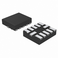
... Semiconductor Components Industries, LLC, 2009 December, 2009 − Rev. 3 ports are designed to track two and V respectively. Both CCB to the output B port Reached 14 at GND NLSV4T244MUTAG NLSV4T244DR2G NLSV4T244DTR2G TSSOP14 †For information on tape and reel specifications, 1 http://onsemi.com MARKING DIAGRAMS UQFN12 URMG MU SUFFIX G CASE 523AE ...

Page 2

CCA GND (Top View PIN ASSIGNMENT PIN FUNCTION V Input Port DC Power Supply CCA V Output Port DC Power Supply CCB ...

Page 3

MAXIMUM RATINGS Symbol Rating Supply Voltage CCA CCB V DC Input Voltage I V Control Input Output Voltage Input Diode Current Output Diode Current ...

Page 4

DC ELECTRICAL CHARACTERISTICS Symbol Parameter V Input HIGH Voltage IH (An, OE) V Input LOW Voltage IL (An, OE) V Output HIGH Voltage OH V Output LOW Voltage OL I Input Leakage Current I I Power−Off Leakage Current OFF I ...

Page 5

TOTAL STATIC POWER CONSUMPTION (I 4.5 V (V) Min Max CCA 4.5 2 3.3 2 2.8 < 2 1.8 < 1 0.9 < 0.5 NOTE: Connect ground before applying supply voltage and V will not damage the ...

Page 6

Pulse Generator Figure 3. AC (Propagation Delay) Test Circuit Test PLH PHL PLZ PZL PHZ PZH equivalent (includes probe and jig capacitance ...

Page 7

... C 0.05 NOTE 3 M 2.30 11X 0.22 *For additional information on our Pb−Free strategy and soldering details, please download the ON Semiconductor Soldering and Mounting Techniques Reference Manual, SOLDERRM/D. http://onsemi.com 7 NOTES: 1. DIMENSIONING AND TOLERANCING PER ASME Y14.5M, 1994. 2. CONTROLLING DIMENSION: MILLIMETERS 3. DIMENSION b APPLIES TO PLATED TERMINAL AND IS MEASURED BETWEEN 0 ...

Page 8

G −T− SEATING 14 PL PLANE 0.25 (0.010 PACKAGE DIMENSIONS SOIC−14 D SUFFIX CASE 751A−03 ISSUE 0.25 (0.010 ...

Page 9

... Opportunity/Affirmative Action Employer. This literature is subject to all applicable copyright laws and is not for resale in any manner. PUBLICATION ORDERING INFORMATION LITERATURE FULFILLMENT: Literature Distribution Center for ON Semiconductor P.O. Box 5163, Denver, Colorado 80217 USA Phone: 303−675−2175 or 800−344−3860 Toll Free USA/Canada Fax: 303− ...

Related keywords