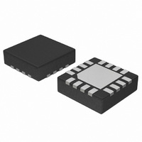
NCN4555MNR2G ON Semiconductor, NCN4555MNR2G Datasheet - Page 8

NCN4555MNR2G
Manufacturer Part Number
NCN4555MNR2G
Description
IC LEVEL SHIFTER SIM CARD 16-QFN
Manufacturer
ON Semiconductor
Datasheet
1.NCN4555MNR2G.pdf
(12 pages)
Specifications of NCN4555MNR2G
Logic Function
Level Shifter
Input Type
Logic
Output Type
Logic
Differential - Input:output
No/No
Voltage - Supply
1.8 V ~ 5.5 V
Operating Temperature
-25°C ~ 85°C
Package / Case
16-TFQFN Exposed Pad
Supply Voltage
1.8 V ~ 5.5 V
Lead Free Status / RoHS Status
Lead free / RoHS Compliant
Number Of Channels
-
Data Rate
-
Other names
NCN4555MNR2G
NCN4555MNR2GOSTR
NCN4555MNR2GOSTR
Available stocks
Company
Part Number
Manufacturer
Quantity
Price
Company:
Part Number:
NCN4555MNR2G
Manufacturer:
ON Semiconductor
Quantity:
500
Part Number:
NCN4555MNR2G
Manufacturer:
ON/安森美
Quantity:
20 000
CARD SUPPLY CONVERTER
Low Dropout Voltage Regulator capable of suppling a
current in excess of 50 mA under 1.8 V or 3.0 V. This device
features a very low quiescent current typically lower than
25 mA (Figure 6 and 7). MOD_V
allowing a logic level signal to select a regulated voltage of
1.8 V (MOD_V
Additionally, the NCN4555 has a shutdown input allowing
it to turn off or turn on the regulator output. The shutdown
mode power consumption is typically in the range of a few
tens of nA (30 nA Typical). Figure 8 shows a simplified
view of the NCN4555 voltage regulator. The SIM_V
output is internally current limited and protected against
short circuits. The short−circuit current IV
over the temperature and SIM_V
typically in the range of 60 mA to 90 mA (Figure 4 and 5).
The NCN4555 interface DC−DC converter is a
CC
STOP
V
= LOW) or 3.0 V (MOD_V
I/O
DD
C
IN
= 0.1 mF
V
BAT
18 k
IO/CONTROL
Figure 8. Simplified Block Diagram of the LDO Voltage Regulator
CC
CC
. It varies with V
Q1
is a select input
Q1
CC
Figure 9. Basic I/O Line Interface
APPLICATION INFORMATION
200 ns
CC
is constant
= HIGH).
http://onsemi.com
LOGIC
I
BAT
lim
CC
−
+
V
REF
8
GND
the LDO the SIM_V
bypass ceramic capacitor to the ground. At the input, V
will be bypassed to the ground with a 0.1 mF ceramic
capacitor.
LEVEL SHIFTERS
that might exist between the microcontroller and the smart
card. The RESET and CLOCK level shifters are
monodirectional and feature both the same architecture.
adapt the voltage difference between the MCU and the SIM
card in both directions. In addition with the pullup resistor,
an active pullup circuit (Figure 8, Q1 and Q2) provides a fast
charge of the stray capacitance, yielding a rise time fully
within the ISO7816 specifications.
200 ns
+
In order to guarantee a stable and satisfying operating of
The level shifters accommodate the voltage difference
The bidirectional I/O line provides a way to automatically
GND
R1
R2
Q2
Q3
GND
CC
14 k
output will be connected to a 1.0 mF
SIM_V
SIM_I/O
C
OUT
SIM_V
CC
= 1.0 mF
MOD_V
CC
CC
BAT


