NLSX3018MUTAG ON Semiconductor, NLSX3018MUTAG Datasheet
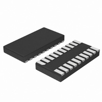
XLATOR DUAL 8BIT CONFIG 20UQFN

NLSX3018MUTAG

Manufacturer Part Number
NLSX3018MUTAG
Description
XLATOR DUAL 8BIT CONFIG 20UQFN
Manufacturer
ON Semiconductor
Datasheet

Specifications of NLSX3018MUTAG

Logic Function
Translator, Bidirectional, 3-State
Number Of Bits
8
Input Type
Voltage
Output Type
Voltage
Data Rate
110Mbps
Number Of Channels
8
Number Of Outputs/channel
1
Differential - Input:output
No/No
Propagation Delay (max)
6.5ns
Voltage - Supply
1.3 V ~ 4.5 V
Operating Temperature
-40°C ~ 85°C
Package / Case
20-UFDFN
Supply Voltage
1.3 V ~ 4.5 V
Lead Free Status / RoHS Status
Lead free / RoHS Compliant

Available stocks

Company
Part Number
Manufacturer
Quantity
Price
Part Number:
NLSX3018MUTAG
Manufacturer:
ON/PBF
Quantity:
16 473
Part Number:
NLSX3018MUTAG
Manufacturer:
ON
Quantity:
3 000
Part Number:
NLSX3018MUTAG
Manufacturer:
ON/安森美
Quantity:
20 000
NLSX3018
8-Bit 100 Mb/s Configurable
Dual-Supply Level
Translator
level translator without a direction control pin. The I/O V
V
and V
to 4.5 V while the V
− 0.4) V. This allows lower voltage logic signals on the V
translated into higher voltage logic signals on the V
vice−versa. Both I/O ports are auto−sensing; thus, no direction pin is
required.
by putting them in 3−state. This significantly reduces the supply
currents from both V
V
Features
Typical Applications
© Semiconductor Components Industries, LLC, 2009
June, 2009 − Rev. 0
L
L
The NLSX3018 is a 8−bit configurable dual−supply bidirectional
The Output Enable (EN) input, when Low, disables both I/O ports
Wide Low−Side V
Wide High−Side V
High−Speed with 100 Mb/s Guaranteed Date Rate for V
Low Bit−to−Bit Skew
Overvoltage Tolerant Enable and I/O Pins
Non−preferential Powerup Sequencing
Small packaging: 4.0 mm x 2.0 mm UQFN20
This is a Pb−Free Device
Mobile Phones, PDAs, Other Portable Devices
−ports are designed to track two different power supply rails, V
.
L
respectively. The V
I/O V
I/O V
I/O V
I/O V
I/O V
I/O V
I/O V
I/O V
EN
V
L
L
L
L
L
L
L
L
1
2
3
4
5
6
7
8
L
10
L
1
2
3
4
5
6
7
8
9
CC
L
PIN ASSIGNMENT
CC
supply rail is configurable from 0.9 V to (V
Operating Range: 0.9 V to (V
and V
Operating Range: 1.3 V to 4.5 V
(Top View)
CC
supply rail is configurable from 1.3 V
L
. The EN signal is designed to track
20
19
18
17
16
15
14
13
12
11
I/O V
I/O V
I/O V
I/O V
V
GND
I/O V
I/O V
I/O V
I/O V
CC
CC
CC
CC
CC
CC
CC
CC
CC
1
2
3
4
5
6
7
8
CC
CC
− 0.4) V
CC
L
side to be
L
side, and
− and I/O
1
> 1.6 V
CC
CC
See detailed ordering and shipping information in the package
dimensions section on page 9 of this data sheet.
(Note: Microdot may be in either location)
ORDERING INFORMATION
A
WL
YY
WW
G
A
L
Y
W
G
LA = Specific Device Code
M
G
http://onsemi.com
= Date Code
= Pb−Free Package
DW SUFFIX
CASE 751D
CASE 517AK
SOIC−20
CASE 948E
DT SUFFIX
TSSOP−20
MU SUFFIX
= Assembly Location
= Wafer Lot
= Year
= Work Week
= Pb−Free Package
= Assembly Location
= Wafer Lot
= Year
= Work Week
= Pb−Free Package
UQFN20
Publication Order Number:
20
1
AWLYYWWG
DIAGRAMS
MARKING
NLSX3018
NLSX3018/D
ALYWG
NLSX
3018
LAM
G
G

Related parts for NLSX3018MUTAG

NLSX3018MUTAG Summary of contents

Page 1

NLSX3018 8-Bit 100 Mb/s Configurable Dual-Supply Level Translator The NLSX3018 is a 8−bit configurable dual−supply bidirectional level translator without a direction control pin. The I −ports are designed to track two different power supply rails and ...

Page 2

Figure 1. Logic Diagram ...

Page 3

NLSX3018 +1.8 V System I I I/ GND EN EN GND Figure 2. Typical Application Circuit PIN ASSIGNMENT Pins Description V V Input ...

Page 4

MAXIMUM RATINGS Symbol Parameter V V Supply Voltage Supply Voltage −Referenced DC Input/Output Voltage −Referenced DC Input/Output Voltage Enable Control Pin DC Input ...

Page 5

DC ELECTRICAL CHARACTERISTICS Symbol Parameter V I/O V Input HIGH IHC CC Voltage V I/O V Input LOW ILC CC Voltage V I/O V Input HIGH IHL L Voltage V I/O V Input LOW ILL L Voltage V Control Pin ...

Page 6

TIMING CHARACTERISTICS Symbol Parameter t I/O V Rise Time R−VCC CC (Output = I/O_V ) CC t I/O V Falltime F−VCC CC (Output = I/O_V ) CC t I/O V Risetime R−VL L (Output = I/O_V ) L t I/O ...

Page 7

ENABLE / DISABLE TIME MEASUREMENTS Symbol Parameter t Turn−On Enable Time (Output = EN−VCC I/O_V , pZH Turn−On Enable Time (Output = I/O_V , pZL t Turn−On Enable Time (Output = EN−VL I/O_V , ...

Page 8

PULSE GENERATOR PZH PHZ PZL PLZ equivalent (Includes jig and probe capacitance OUT Figure 6. Test Circuit for Enable/Disable ...

Page 9

... I/O pins. Driving the Enable pin to a low logic level minimizes the power consumption of ORDERING INFORMATION Device NLSX3018MUTAG NLSX3018DTR2G NLSX3018DWR2G †For information on tape and reel specifications, including part orientation and tape sizes, please refer to our Tape and Reel Packaging Specifications Brochure, BRD8011/D ...

Page 10

... M NOTE 3 C 0.05 M 0.88 *For additional information on our Pb−Free strategy and soldering details, please download the ON Semiconductor Soldering and Mounting Techniques Reference Manual, SOLDERRM/D. http://onsemi.com 10 NOTES: 1. DIMENSIONING AND TOLERANCING PER ASME Y14.5M, 1994. 2. CONTROLLING DIMENSION: MILLIMETERS. 3. DIMENSIONS b APPLIES TO PLATED TERMINAL AND IS MEASURED BETWEEN 0 ...

Page 11

K 20X REF 0.10 (0.004) 0.15 (0.006 L PIN 1 IDENT 1 0.15 (0.006 −V− 0.100 (0.004) −T− SEATING PLANE 16X 0.36 PACKAGE DIMENSIONS TSSOP−20 CASE 948E−02 ...

Page 12

... SCILLC is an Equal Opportunity/Affirmative Action Employer. This literature is subject to all applicable copyright laws and is not for resale in any manner. PUBLICATION ORDERING INFORMATION LITERATURE FULFILLMENT: Literature Distribution Center for ON Semiconductor P.O. Box 5163, Denver, Colorado 80217 USA Phone: 303−675−2175 or 800−344−3860 Toll Free USA/Canada Fax: 303− ...

Related keywords