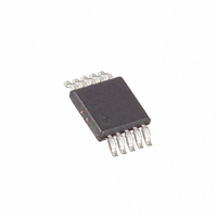
MAX9376EUB+T Maxim Integrated Products, MAX9376EUB+T Datasheet - Page 6

MAX9376EUB+T
Manufacturer Part Number
MAX9376EUB+T
Description
IC TRANSLATOR DUAL 10-UMAX
Manufacturer
Maxim Integrated Products
Datasheet
1.MAX9376EUB.pdf
(8 pages)
Specifications of MAX9376EUB+T
Logic Function
Translator
Number Of Bits
2
Input Type
AnyLevel™
Output Type
LVDS, LVPECL
Number Of Channels
2
Number Of Outputs/channel
2
Differential - Input:output
Yes/No
Voltage - Supply
3 V ~ 3.6 V
Operating Temperature
-40°C ~ 85°C
Package / Case
10-MSOP, Micro10™, 10-uMAX, 10-uSOP
Supply Voltage
3 V ~ 3.6 V
Lead Free Status / RoHS Status
Lead free / RoHS Compliant
Data Rate
-
LVDS/Anything-to-LVPECL/LVDS Dual Translator
Figure 1. Input Definition
Figure 2. LVDS Output Load and Transition Times
Figure 3. Differential Input-to-Output Propagation Delay Timing
Diagram
6
OUT2 - OUT2
OUT
OUT
OUT - OUT
IN
IN
_______________________________________________________________________________________
DIFFERENTIAL OUTPUT
GND
V
CC
WAVEFORM
VOD(-)
DRV
V
V
ID
ID
20%
t
PLH
C
20%
80%
L
V
OUT2
OUT2
ID
t
R
OR (V
t
R
+V
IH
-V
V
OD
OD
OD
- V
80%
IL
OR (V
OR +(V
OR -(V
)
C
VOD(+)
L
OH
OH
OH
VOD
- V
- V
- V
OL
OL
OL
80%
)
t
0V DIFFERENTIAL
)
PHL
)
R
R
L
L
/ 2
/ 2
t
F
80%
t
V
V
F
CM
CM
0V DIFFERENTIAL
GND
(MIN)
20%
(MAX)
20%
V
V
OH
OL
VOS
0V
Terminate the MAX9376 LVPECL outputs with 50Ω to
(V
Terminate OUT1 and OUT1 with identical termination
on each for low output distortion. When a single-ended
signal is taken from the differential output, terminate
both OUT1 and OUT1.
Ensure that output currents do not exceed the current
limits as specified in the Absolute Maximum Ratings .
Under all operating conditions, the device’s total ther-
mal limits should be observed.
The MAX9376 LVDS outputs are current-steering
devices; no output voltage is generated without a termi-
nation resistor. The termination resistors should match
the differential impedance of the transmission line.
Output voltage levels are dependent upon the value of
the termination resistor. The MAX9376 is optimized for
point-to-point interface with 100Ω termination resistors
at the receiver inputs. Termination resistance values
may range between 90Ω and132Ω, depending on the
characteristic impedance of the transmission medium.
Bypass V
mount ceramic 0.1µF and 0.01µF capacitors. Place the
capacitors as close to the device as possible with the
0.01µF capacitor closest to the device pins.
Circuit board trace layout is very important to maintain
the signal integrity of high-speed differential signals.
Maintaining integrity is accomplished in part by reduc-
ing signal reflections and skew, and increasing com-
mon-mode noise immunity.
Signal reflections are caused by discontinuities in the
50Ω characteristic impedance of the traces. Avoid dis-
continuities by maintaining the distance between differ-
ential traces, not using sharp corners or using vias.
Maintaining distance between the traces also increases
common-mode noise immunity. Reducing signal skew
is accomplished by matching the electrical length of
the differential traces.
CC
- 2V) or use equivalent Thevenin terminations.
CC
to ground with high-frequency surface-
Applications Information
LVPECL Output Termination
LVDS Output Termination
Supply Bypassing
Traces


