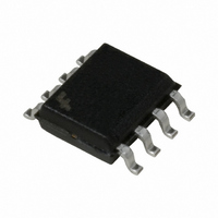
100LVELT22M Fairchild Semiconductor, 100LVELT22M Datasheet - Page 2

100LVELT22M
Manufacturer Part Number
100LVELT22M
Description
TRANSLATOR 3.3V DUAL DIFF 8SOIC
Manufacturer
Fairchild Semiconductor
Series
100LVELr
Datasheet
1.100LVELT22M.pdf
(5 pages)
Specifications of 100LVELT22M
Logic Function
Translator
Number Of Bits
2
Input Type
LVTTL/LVCMOS
Output Type
LVPECL
Number Of Channels
2
Number Of Outputs/channel
1
Differential - Input:output
Yes/No
Propagation Delay (max)
0.35ns
Voltage - Supply
3 V ~ 3.8 V
Operating Temperature
-40°C ~ 85°C
Package / Case
8-SOIC (3.9mm Width)
Supply Voltage
3 V ~ 3.8 V
Lead Free Status / RoHS Status
Lead free / RoHS Compliant
Data Rate
-
www.fairchildsemi.com
I
V
V
f
t
t
t
t
I
I
V
V
V
CC
MAX
JITTER
PLH
SKEW
r
Absolute Maximum Ratings
LVPECL DC Electrical Characteristics
Note 2: Output parameters vary 1 to 1 with V
Note 3: Outputs are terminated through a 50
Note: Devices are designed to meet the DC specifications after thermal equilibrium has been established. Circuit is tested with air flow greater than
500LFPM maintained.
LVTTL/LVCMOS DC Electrical Characteristics
IH
IL
Note 4: V
Note: Devices are designed to meet the DC specifications after thermal equilibrium has been established. Circuit is tested with air flow greater than
500LFPM maintained.
AC Electrical Characteristics
Note 5: V
Note 6: Specifications for standard LVTTL input signal (see Figure 1).
Symbol
, t
OH
OL
Supply Voltage (V
Input Voltage (V
DC Output Current (I
Storage Temperature (T
IK
IH
IL
Symbol
Symbol
f
Continuous
Surge
/ t
PHL
CC
CC
Power Supply Current
Output HIGH Voltage (Note 3)
Output LOW Voltage (Note 3)
can vary 0.15V.
can vary 0.15V.
Maximum Toggle Frequency
Cycle-to-Cycle Jitter
Propagation Delay (Note 6)
Skew
Output Rise Time Q (20% to 80%)
Input HIGH Current
Input LOW Current
Clamp Diode Voltage
Input HIGH Voltage
Input LOW Voltage
I
) V
CC
Output-to-Output
Part-to-Part
I
Parameter
)
OUT
Parameter
V
CC
STG
Parameter
)
)
CC
resistor to V
. V
CC
can vary 0.15V.
Min
200
200
65 C to 150 C
0.0V to 7.0V
0.0V to 7.0V
CC
(Note 1)
2215
1470
Min
V
2.0V.
TBD
TBD
40 C
Typ
350
CC
30
100 mA
Min
50 mA
2.0
40 C
Typ
3.3V; GND
T
A
Max
600
100
400
550
2
40 C to 85 C
2420
1745
Max
Recommended Operating
Conditions
Note 1: The “Absolute Maximum Ratings” are those values beyond which
the safety of the device cannot be guaranteed. The device should not be
operated at these limits. The parametric values defined in the Electrical
Characteristics tables are not guaranteed at the absolute maximum rating.
The “Recommended Operating Conditions” table will define the conditions
for actual device operation.
28
Typ
Power Supply Operating
LVTTL/LVCMOS Input Voltage
Free Air Operating Temperature (T
V
CC
Min
200
200
0.0V (Note 5)
2275
1490
3.3V; GND
Min
25 C
TBD
TBD
Max
Typ
350
100
0.8
30
20
200
1.2
V
25 C
CC
Typ
Max
600
100
400
500
Units
3.3V; GND
0.0V (Note 2)
V
V
V
A
A
2420
1680
Max
28
Min
200
200
V
V
V
I
IN
IN
IN
IN
2275
1490
Min
85 C
2.7V
V
0.5V
TBD
TBD
0.0V (Note 4)
18 mA
Typ
350
30
CC
A
)
85 C
Typ
Condition
V
Max
600
100
400
500
CC
40 C to 85 C
3.0V to 3.8V
2420
1680
Units
0.0V to V
Max
MHz
29
ps
ps
ps
ns
Figure
Number
Figure 1
Figure 2
Units
mA
mV
mV
CC


