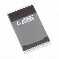
AT49F001-55VI Atmel, AT49F001-55VI Datasheet - Page 2

AT49F001-55VI
Manufacturer Part Number
AT49F001-55VI
Description
IC FLASH 1MBIT 55NS 32VSOP
Manufacturer
Atmel
Datasheet
1.AT49F001-55VC.pdf
(22 pages)
Specifications of AT49F001-55VI
Format - Memory
FLASH
Memory Type
FLASH
Memory Size
1M (128K x 8)
Speed
55ns
Interface
Parallel
Voltage - Supply
4.5 V ~ 5.5 V
Operating Temperature
-40°C ~ 85°C
Package / Case
32-VSOP
Lead Free Status / RoHS Status
Contains lead / RoHS non-compliant
Block Diagram
2
AT49F001(N(T)
55 ns with power dissipation of just 275 mW over the commercial temperature range. When
the device is deselected, the CMOS standby current is less than 100 A. For the
AT49F001N(T) pin 1 for the DIP and PLCC packages and pin 9 for the TSOP package are
don’t connect pins.
To allow for simple in-system reprogrammability, the AT49F001(N)(T) does not require high
input voltages for programming. Five-volt-only commands determine the read and program-
ming operation of the device. Reading data out of the device is similar to reading from an
EPROM; it has standard CE, OE, and WE inputs to avoid bus contention. Reprogramming the
AT49F001(N)(T) is performed by erasing a block of data and then programming on a byte-by-
byte basis. The byte programming time is a fast 50 µs. The end of a program cycle can be
optionally detected by the DATA polling feature. Once the end of a byte program cycle has
been detected, a new access for a read or program can begin. The typical number of program
and erase cycles is in excess of 10,000 cycles.
The device is erased by executing the erase command sequence; the device internally con-
trols the erase operations. There are two 8K bytes parameter block sections and two main
memory blocks.
The device has the capability to protect the data in the boot block; this feature is enabled by a
command sequence. The 16-Kbyte boot block section includes a reprogramming lock out fea-
ture to provide data integrity. The boot sector is designed to contain user secure code, and
when the feature is enabled, the boot sector is protected from being reprogrammed.
In the AT49F001(N)(T), once the boot block programming lockout feature is enabled, the con-
tents of the boot block are permanent and cannot be changed. In the AT49F001(T), once the
boot block programming lockout feature is enabled, the contents of the boot block cannot be
changed with input voltage levels of 5.5 volts or less.
ADDRESS
INPUTS
RESET
GND
VCC
WE
OE
CE
Y DECODER
X DECODER
CONTROL
LOGIC
DATA INPUTS/OUTPUTS
DATA LATCHES
INPUT/OUTPUT
MAIN MEMORY
MAIN MEMORY
BOOT BLOCK
PARAMETER
PARAMETER
AT49F001(N)
(64K BYTES)
(32K BYTES)
(16K BYTES)
(8K BYTES)
(8K BYTES)
PROGRAM
Y-GATING
I/O7 - I/O0
BUFFERS
BLOCK 2
BLOCK 1
BLOCK 2
BLOCK 1
8
1FFFF
10000
0FFFF
08000
07FFF
06000
05FFF
04000
03FFF
00000
DATA INPUTS/OUTPUTS
DATA LATCHES
INPUT/OUTPUT
MAIN MEMORY
MAIN MEMORY
AT49F001(N)T
BOOT BLOCK
PARAMETER
PARAMETER
(16K BYTES)
(32K BYTES)
(64K BYTES)
(8K BYTES)
(8K BYTES)
PROGRAM
Y-GATING
I/O7 - I/O0
BUFFERS
BLOCK 1
BLOCK 2
BLOCK 1
BLOCK 2
1008D–FLASH–2/03
8
1FFFF
1C000
1BFFF
1A000
19FFF
18000
17FFF
10000
0FFFF
00000


