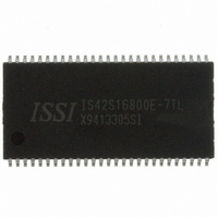
IS42S16800E-7TL ISSI, Integrated Silicon Solution Inc, IS42S16800E-7TL Datasheet - Page 26

IS42S16800E-7TL
Manufacturer Part Number
IS42S16800E-7TL
Description
IC SDRAM 128MBIT 143MHZ 54TSOP
Manufacturer
ISSI, Integrated Silicon Solution Inc
Type
SDRAMr
Datasheet
1.IS42S81600E-7TL.pdf
(61 pages)
Specifications of IS42S16800E-7TL
Package / Case
54-TSOP II
Memory Size
128M (8Mx16)
Format - Memory
RAM
Memory Type
SDRAM
Speed
143MHz
Interface
Parallel
Voltage - Supply
3 V ~ 3.6 V
Operating Temperature
0°C ~ 70°C
Data Bus Width
8 bit
Organization
8 Mbit x 16
Maximum Clock Frequency
143 MHz
Access Time
7 ns
Supply Voltage (max)
3.6 V
Supply Voltage (min)
3 V
Maximum Operating Current
120 mA
Maximum Operating Temperature
+ 70 C
Minimum Operating Temperature
0 C
Mounting Style
SMD/SMT
Density
128Mb
Address Bus
14b
Access Time (max)
6.5/5.4ns
Maximum Clock Rate
143MHz
Operating Supply Voltage (typ)
3.3V
Package Type
TSOP-II
Operating Temp Range
0C to 70C
Operating Supply Voltage (max)
3.6V
Operating Supply Voltage (min)
3V
Supply Current
130mA
Pin Count
54
Mounting
Surface Mount
Operating Temperature Classification
Commercial
Lead Free Status / RoHS Status
Lead free / RoHS Compliant
Lead Free Status / RoHS Status
Lead free / RoHS Compliant, Lead free / RoHS Compliant
Other names
706-1064
IS42S16800E-7TL
IS42S16800E-7TL
Available stocks
Company
Part Number
Manufacturer
Quantity
Price
Company:
Part Number:
IS42S16800E-7TL
Manufacturer:
ISSI
Quantity:
1 000
Company:
Part Number:
IS42S16800E-7TL
Manufacturer:
ISSI
Quantity:
1 000
Company:
Part Number:
IS42S16800E-7TL
Manufacturer:
GSI
Quantity:
655
Part Number:
IS42S16800E-7TL
Manufacturer:
ISSI
Quantity:
20 000
Company:
Part Number:
IS42S16800E-7TLI
Manufacturer:
ISSI
Quantity:
3 520
Company:
Part Number:
IS42S16800E-7TLI
Manufacturer:
ISSI
Quantity:
2 148
Part Number:
IS42S16800E-7TLI
Manufacturer:
ISSI
Quantity:
20 000
CAS LATENCY
three clocks.
the latency is m clocks, the data will be available by clock
edge n + m. The DQs will start driving as a result of the
clock edge one cycle earlier (n + m - 1), and provided that
the relevant access times are met, the data will be valid by
clock edge n + m. For example, assuming that the clock
cycle time is such that all relevant access times are met,
if a READ command is registered at T0 and the latency
is programmed to two clocks, the DQs will start driving
after T1 and the data will be valid by T2, as shown in CAS
Latency diagrams. The Allowable Operating Frequency
table indicates the operating frequencies at which each
CAS latency setting can be used.
Reserved states should not be used as unknown operation
or incompatibility with future versions may result.
IS42S81600E, IS42S16800E
CAS Latency
The CAS latency is the delay, in clock cycles, between
the registration of a READ command and the availability of
the first piece of output data. The latency can be set to two or
If a READ command is registered at clock edge n, and
26
COMMAND
COMMAND
CLK
CLK
DQ
DQ
READ
READ
T0
T0
CAS Latency - 2
NOP
NOP
CAS Latency - 3
T1
T1
t
LZ
t
AC
CAS Latency
applies to both READ and WRITE bursts; when M9 = 1,
write accesses are single-location (nonburst) accesses.
Operating Mode
The normal operating mode is selected by setting M7 and M8
to zero; the other combinations of values for M7 and M8 are
reserved for future use and/or test modes. The programmed
burst length applies to both READ and WRITE bursts.
Test modes and reserved states should not be used be-
cause unknown operation or incompatibility with future
versions may result.
Write Burst Mode
When M9 = 0, the burst length programmed via M0-M2
the programmed burst length applies to READ bursts, but
Speed
-75E
NOP
NOP
Allowable Operating Frequency (MHz)
-5
-6
-7
T2
T2
Integrated Silicon Solution, Inc. — www.issi.com
D
OUT
t
t
OH
LZ
t
AC
NOP
T3
T3
CAS Latency = 2
D
DON'T CARE
UNDEFINED
OUT
t
OH
100
100
100
133
T4
CAS Latency = 3
200
166
143
—
03/16/2011
Rev. D


