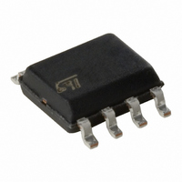
M93C86-WMN6P STMicroelectronics, M93C86-WMN6P Datasheet - Page 15

M93C86-WMN6P
Manufacturer Part Number
M93C86-WMN6P
Description
IC EEPROM 16KBIT 2MHZ 8SOIC
Manufacturer
STMicroelectronics
Datasheets
1.M93C46-WMN6TP.pdf
(36 pages)
2.M93C46-WMN6TP.pdf
(37 pages)
3.M93C46-WBN6P.pdf
(31 pages)
Specifications of M93C86-WMN6P
Format - Memory
EEPROMs - Serial
Memory Type
EEPROM
Memory Size
16K (2K x 8 or 1K x 16)
Speed
2MHz
Interface
Microwire, 3-Wire Serial
Voltage - Supply
2.5 V ~ 5.5 V
Operating Temperature
-40°C ~ 85°C
Package / Case
8-SOIC (3.9mm Width)
Organization
2 K x 8
Interface Type
Microwire
Maximum Clock Frequency
2 MHz
Supply Voltage (max)
5.5 V
Supply Voltage (min)
2.5 V
Maximum Operating Current
2 mA
Maximum Operating Temperature
+ 85 C
Mounting Style
SMD/SMT
Minimum Operating Temperature
- 40 C
Operating Supply Voltage
2.5 V, 5.5 V
Memory Configuration
2048 X 8, 1024 X 16
Clock Frequency
2MHz
Supply Voltage Range
2.5V To 5.5V
Memory Case Style
SOIC
No. Of Pins
8
Rohs Compliant
Yes
Lead Free Status / RoHS Status
Lead free / RoHS Compliant
Other names
497-4927-5
M93C86, M93C76, M93C66, M93C56, M93C46
5.3
Figure 4.
1. For the meanings of An, Xn, Qn and Dn, see
Erase Byte or Word
The Erase Byte or Word (ERASE) instruction sets the bits of the addressed memory byte (or
word) to 1. Once the address has been correctly decoded, the falling edge of the Chip
Select Input (S) starts the self-timed Erase cycle. The completion of the cycle can be
detected by monitoring the READY/BUSY line, as described in the
section.
Read
Write
Write
Enable
READ, WRITE, WEN, WDS sequences
S
Q
S
S
Q
D
D
D
1 0
1
1 1 0 An
CODE
CODE
CODE
OP
0
OP
OP
1
0
1
An
1
ADDR
ADDR
Doc ID 4997 Rev 11
Xn X0
A0
A0
Qn
Dn
Table
5.,
DATA OUT
DATA IN
Table 6.
Write
Disable
and
Table
S
D
D0
Q0
7..
BUSY
READY/BUSY status
1
CODE
STATUS
CHECK
0
OP
0
0
0
READY
Xn X0
Instructions
AI00878d
15/36


