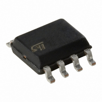
M95M01-RMN6TP STMicroelectronics, M95M01-RMN6TP Datasheet - Page 10

M95M01-RMN6TP
Manufacturer Part Number
M95M01-RMN6TP
Description
IC EEPROM 1MBIT 5MHZ 8SOIC
Manufacturer
STMicroelectronics
Datasheet
1.M95M01-RMN6TP.pdf
(41 pages)
Specifications of M95M01-RMN6TP
Format - Memory
EEPROMs - Serial
Memory Type
EEPROM
Memory Size
1M (128K x 8)
Speed
5MHz
Interface
SPI, 3-Wire Serial
Voltage - Supply
1.8 V ~ 5.5 V
Operating Temperature
-40°C ~ 85°C
Package / Case
8-SOIC (3.9mm Width)
Organization
128 K x 8
Interface Type
SPI
Maximum Clock Frequency
5 MHz
Access Time
80 ns
Supply Voltage (max)
5.5 V
Supply Voltage (min)
1.8 V
Maximum Operating Current
5 mA
Maximum Operating Temperature
+ 85 C
Mounting Style
SMD/SMT
Minimum Operating Temperature
- 40 C
Operating Supply Voltage
2.5 V, 3.3 V, 5 V
Lead Free Status / RoHS Status
Lead free / RoHS Compliant
Other names
497-8701-2
M95M01-RMN6TP
M95M01-RMN6TP
Available stocks
Company
Part Number
Manufacturer
Quantity
Price
Company:
Part Number:
M95M01-RMN6TP
Manufacturer:
INFINEON
Quantity:
23
Company:
Part Number:
M95M01-RMN6TP
Manufacturer:
STMicroelectronics
Quantity:
76 802
Part Number:
M95M01-RMN6TP
Manufacturer:
ST
Quantity:
20 000
Connecting to the SPI bus
3
10/41
Connecting to the SPI bus
These devices are fully compatible with the SPI protocol.
All instructions, addresses and input data bytes are shifted in to the device, most significant
bit first. The Serial Data Input (D) is sampled on the first rising edge of the Serial Clock (C)
after Chip Select (S) goes low.
All output data bytes are shifted out of the device, most significant bit first. The Serial Data
Output (Q) is latched on the first falling edge of the Serial Clock (C) after the instruction
(such as the Read from Memory Array and Read Status Register instructions) have been
clocked into the device.
Figure 4.
1. The Write Protect (W) and Hold (HOLD) signals should be driven high or low as appropriate.
Figure 4
Only one device is selected at a time, so only one device drives the Serial Data Output (Q)
line at a time, the other devices are high impedance.
The pull-up resistor R (represented in
master leaves the S line in the high impedance state.
In applications where the bus master might enter a state where the whole input/output SPI
bus is high-impedance at a given time (for example, if the bus master is reset during the
transmission of an instruction), the clock line (C) must be connected to an external pull-
down resistor so that, if all inputs/outputs become high impedance, the C line is pulled low
(while the S line is pulled high). This ensures that S and C do not become high at the same
time, and so, that the t
SPI Interface with
(CPOL, CPHA) =
CS3
(0, 0) or (1, 1)
SPI Bus Master
CS2 CS1
shows an example of three memory devices connected to an MCU, on an SPI bus.
Bus master and memory devices on the SPI bus
SDO
SDI
SCK
R
SHCH
R
requirement is met. The typical value of R is 100 k.
C Q D
S
Doc ID 13264 Rev 7
SPI Memory
Device
W
Figure
V
CC
HOLD
V
R
4) ensures that no device is selected if the bus
SS
C Q D
S
SPI Memory
Device
W
V
HOLD
CC
V
R
SS
M95M01-R, M95M01-W
C Q D
S
SPI Memory
Device
W
V
CC
HOLD
AI12836b
V
SS
V
V
CC
SS


