CY7C1049DV33-10VXI Cypress Semiconductor Corp, CY7C1049DV33-10VXI Datasheet - Page 5
CY7C1049DV33-10VXI
Manufacturer Part Number
CY7C1049DV33-10VXI
Description
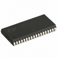
IC SRAM 4MBIT 10NS 36SOJ
Manufacturer
Cypress Semiconductor Corp
Type
Asynchronousr
Datasheet
1.CY7C1049DV33-10VXI.pdf
(11 pages)
Specifications of CY7C1049DV33-10VXI
Memory Size
4M (512K x 8)
Package / Case
36-SOJ
Format - Memory
RAM
Memory Type
SRAM - Asynchronous
Speed
10ns
Interface
Parallel
Voltage - Supply
3 V ~ 3.6 V
Operating Temperature
-40°C ~ 85°C
Access Time
10 ns
Supply Voltage (max)
3.6 V
Supply Voltage (min)
3 V
Maximum Operating Current
90 mA
Maximum Operating Temperature
+ 85 C
Minimum Operating Temperature
- 40 C
Mounting Style
SMD/SMT
Number Of Ports
1
Operating Supply Voltage
3.3 V
Memory Configuration
512K X 8
Supply Voltage Range
3V To 3.6V
Memory Case Style
SOJ
No. Of Pins
36
Operating Temperature Range
-40°C To +85°C
Rohs Compliant
Yes
Lead Free Status / RoHS Status
Lead free / RoHS Compliant
Lead Free Status / RoHS Status
Lead free / RoHS Compliant, Lead free / RoHS Compliant
Other names
428-1981-5
CY7C1049DV33-10VXI
CY7C1049DV33-10VXI
Available stocks
Company
Part Number
Manufacturer
Quantity
Price
Company:

Part Number:
CY7C1049DV33-10VXI
Manufacturer:
CY
Quantity:
6 250
Part Number:
CY7C1049DV33-10VXI
Manufacturer:
CYPRESS/赛普拉斯
Quantity:
20 000
Company:
Part Number:
CY7C1049DV33-10VXIT
Manufacturer:
CYPRESS
Quantity:
2 100
Company:
Part Number:
CY7C1049DV33-10VXIT
Manufacturer:
CY
Quantity:
6 250
Company:
Part Number:
CY7C1049DV33-10VXIT
Manufacturer:
CYPRESS/PBF
Quantity:
146
Part Number:
CY7C1049DV33-10VXIT
Manufacturer:
专营CYPRESS
Quantity:
20 000


AC Switching Characteristics
Over the Operating Range
Notes
Document Number: 38-05475 Rev. *F
Read Cycle
t
t
t
t
t
t
t
t
t
t
t
t
Write Cycle
t
t
t
t
t
t
t
t
t
t
7. Test conditions assume signal transition time of 3 ns or less, timing reference levels of 1.5V, input pulse levels of 0 to 3.0V, and output loading of the specified I
8. t
9. t
10. At any temperature and voltage condition, t
11. The internal write time of the memory is defined by the overlap of CE LOW, and WE LOW. CE and WE must be LOW to initiate a write, and the transition of either of these signals
12. The minimum write cycle time for Write Cycle No. 2 (WE controlled, OE LOW) is the sum of t
power
RC
AA
OHA
ACE
DOE
LZOE
HZOE
LZCE
HZCE
PU
PD
WC
SCE
AW
HA
SA
PWE
SD
HD
LZWE
HZWE
Parameter
and 30 pF load capacitance.
can terminate the write. The input data set up and hold timing must be referred to the leading edge of the signal that terminates the write.
POWER
HZOE
[8]
, t
HZCE
gives the minimum amount of time that the power supply must be at stable, typical V
, and t
[11, 12]
V
Read Cycle Time
Address to Data Valid
Data Hold from Address Change
CE LOW to Data Valid
OE LOW to Data Valid
OE LOW to Low Z
OE HIGH to High Z
CE LOW to Low Z
CE HIGH to High-Z
CE LOW to Power up
CE HIGH to Power down
Write Cycle Time
CE LOW to Write End
Address Set up to Write End
Address Hold from Write End
Address Set up to Write Start
WE Pulse Width
Data Set up to Write End
Data Hold from Write End
WE HIGH to Low Z
WE LOW to High Z
CC
HZWE
(typical) to the first access
are specified with a load capacitance of 5 pF as in part (d) of AC Test Loads. Transition is measured when the outputs enter a high impedance state.
[7]
[10]
[10]
[9, 10]
[9, 10]
[9, 10]
HZCE
Description
is less than t
LZCE
, t
HZOE
is less than t
LZOE
, and t
HZWE
CC
HZWE
values until the first memory access is performed.
-10 (Industrial)
Min
100
is less than t
10
10
3
0
3
0
7
7
0
0
7
5
0
3
and t
SD
.
LZWE
Max
10
10
10
5
5
5
5
for any given device.
-12 (Automotive)
Min
100
12
12
3
0
3
0
8
8
0
0
8
6
0
3
CY7C1049DV33
Max
12
12
12
6
6
6
6
Page 5 of 11
Unit
s
ns
ns
ns
ns
ns
ns
ns
ns
ns
ns
ns
ns
ns
ns
ns
ns
ns
ns
ns
ns
ns
OL
/I
OH
[+] Feedback
Related parts for CY7C1049DV33-10VXI
Image
Part Number
Description
Manufacturer
Datasheet
Request
R

Part Number:
Description:
17ns, 512Kx8 static RAM (SRAM)
Manufacturer:
Cypress Semiconductor Corporation.
Datasheet:
Part Number:
Description:
20ns, 512Kx8 static RAM (SRAM)
Manufacturer:
Cypress Semiconductor Corporation.
Datasheet:
Part Number:
Description:
20ns, 512Kx8 static RAM (SRAM)
Manufacturer:
Cypress Semiconductor Corporation.
Datasheet:
Part Number:
Description:
15ns, 512Kx8 static RAM (SRAM)
Manufacturer:
Cypress Semiconductor Corporation.
Datasheet:
Part Number:
Description:
25ns, 512Kx8 static RAM (SRAM)
Manufacturer:
Cypress Semiconductor Corporation.
Datasheet:

Part Number:
Description:
512K x 8 Static RAM
Manufacturer:
CYPRESS [Cypress Semiconductor]
Datasheet:

Part Number:
Description:
Manufacturer:
Cypress Semiconductor Corp
Datasheet:
Part Number:
Description:
Manufacturer:
Cypress Semiconductor Corp
Datasheet: