CY7C1021BN-15VXE Cypress Semiconductor Corp, CY7C1021BN-15VXE Datasheet - Page 3
CY7C1021BN-15VXE
Manufacturer Part Number
CY7C1021BN-15VXE
Description
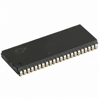
IC SRAM 1MBIT 15NS 44SOJ
Manufacturer
Cypress Semiconductor Corp
Type
Asynchronousr
Datasheet
1.CY7C1021BNL-15ZXI.pdf
(13 pages)
Specifications of CY7C1021BN-15VXE
Memory Size
1M (64K x 16)
Package / Case
44-SOJ
Format - Memory
RAM
Memory Type
SRAM - Asynchronous
Speed
15ns
Interface
Parallel
Voltage - Supply
4.5 V ~ 5.5 V
Operating Temperature
-40°C ~ 125°C
Access Time
15 ns
Supply Voltage (max)
5.5 V
Supply Voltage (min)
4.5 V
Maximum Operating Current
130 mA
Maximum Operating Temperature
+ 125 C
Minimum Operating Temperature
- 40 C
Mounting Style
SMD/SMT
Number Of Ports
1
Operating Supply Voltage
5 V
Lead Free Status / RoHS Status
Lead free / RoHS Compliant
Lead Free Status / RoHS Status
Lead free / RoHS Compliant, Lead free / RoHS Compliant


Selection Guide
Pin Configuration
Pin Definitions
Document #: 001-06494 Rev. *C
Maximum access time (ns)
Maximum operating current (mA)
Maximum CMOS standby current (mA) Commercial/Industrial
Pin Name
I/O
BHE, BLE
A
0
1
V
V
WE
NC
CE
OE
–A
–I/O
SS
CC
15
16
1–5,18–21, 24–27, 42–44
7–10, 13–16, 29–32,
Pin Number
22, 23, 28
35–38
40, 39
12, 34
11, 33
17
41
6
Description
Commercial/Industrial
Automotive-A
Automotive-E
Commercial/Industrial (L version)
Automotive-A (L version)
Automotive-E
Power Supply Power supply inputs to the device.
Input/Control Write enable input, active LOW. When selected LOW, a write is
Input/Control Chip enable input, active LOW. When LOW, selects the chip. When HIGH,
Input/Control Byte enable select inputs, active LOW. BHE controls I/O
Input/Control Output enable, active LOW. Controls the direction of the I/O pins. When
Input/Output Bidirectional data I/O lines. Used as input or output lines depending on
No Connect Not connected to the die.
Figure 1. 44-Pin SOJ/TSOP II (Top View)
I/O Type
Ground
Input
I/O
I/O
I/O
I/O
V
I/O
I/O
I/O
I/O
V
A
A
A
A
WE
NC
CE
CC
A
A
A
A
A
SS
15
14
13
12
4
3
2
1
0
1
2
3
4
5
6
7
8
Address inputs used to select one of the address locations.
operation.
conducted. When deselected HIGH, a read is conducted.
deselects the chip.
controls I/O
LOW, the I/O pins are allowed to behave as outputs. When deasserted
HIGH, I/O pins are tristated, and act as input data pins.
Ground for the device. Should be connected to ground of the system.
13
14
15
16
17
18
19
20
21
22
1
2
3
4
5
6
7
8
9
10
11
12
44
43
42
41
40
39
38
37
36
35
34
33
32
31
30
29
28
27
26
25
24
23
8
–I/O
A
A
A
OE
BHE
BLE
I/O
I/O
I/O
I/O
V
V
I/O
I/O
I/O
I/O
NC
A
A
A
A
NC
5
6
7
SS
CC
8
9
10
11
1
16
15
14
13
12
11
10
9
.
CY7C10211B-10 CY7C1021B-12 CY7C1021B-15
CY7C1021BN, CY7C10211BN
150
0.5
10
10
-
-
-
-
Description
140
0.5
12
10
-
-
-
-
Page 3 of 13
16
–I/O
130
130
130
0.5
0.5
15
10
15
9
, BLE
[+] Feedback
Related parts for CY7C1021BN-15VXE
Image
Part Number
Description
Manufacturer
Datasheet
Request
R

Part Number:
Description:
CY7C1021BN-15ZSXE
Manufacturer:
Cypress Semiconductor Corp
Datasheet:
Part Number:
Description:
IC SRAM 1MBIT 15NS 44TSOP
Manufacturer:
Cypress Semiconductor Corp
Datasheet:

Part Number:
Description:
CY7C1021BN-15VXET
Manufacturer:
Cypress Semiconductor Corp
Datasheet:
Part Number:
Description:
CY7C1021BN-15ZSXET
Manufacturer:
Cypress Semiconductor Corp
Datasheet:
Part Number:
Description:
IC SRAM 1MBIT 12NS 44SOJ
Manufacturer:
Cypress Semiconductor Corp
Datasheet:
Part Number:
Description:
IC SRAM 1MBIT 12NS 44SOJ
Manufacturer:
Cypress Semiconductor Corp
Datasheet:
Part Number:
Description:
IC SRAM 1MBIT 12NS 44SOJ
Manufacturer:
Cypress Semiconductor Corp
Datasheet:
Part Number:
Description:
IC SRAM 1MBIT 12NS 44SOJ
Manufacturer:
Cypress Semiconductor Corp
Datasheet:
Part Number:
Description:
IC SRAM 1MBIT 12NS 44TSOP
Manufacturer:
Cypress Semiconductor Corp
Datasheet:
Part Number:
Description:
IC SRAM 1MBIT 12NS 44TSOP
Manufacturer:
Cypress Semiconductor Corp
Datasheet:
Part Number:
Description:
IC SRAM 1MBIT 15NS 44SOJ
Manufacturer:
Cypress Semiconductor Corp
Datasheet:
Part Number:
Description:
IC SRAM 1MBIT 15NS 44SOJ
Manufacturer:
Cypress Semiconductor Corp
Datasheet:
Part Number:
Description:
IC SRAM 1MBIT 15NS 44SOJ
Manufacturer:
Cypress Semiconductor Corp
Datasheet:
Part Number:
Description:
IC SRAM 1MBIT 15NS 44SOJ
Manufacturer:
Cypress Semiconductor Corp
Datasheet:
Part Number:
Description:
IC SRAM 1MBIT 15NS 44TSOP
Manufacturer:
Cypress Semiconductor Corp
Datasheet: