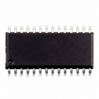
M48Z35Y-70MH1E STMicroelectronics, M48Z35Y-70MH1E Datasheet - Page 9

M48Z35Y-70MH1E
Manufacturer Part Number
M48Z35Y-70MH1E
Description
IC NVSRAM 256KBIT 70NS 28SOIC
Manufacturer
STMicroelectronics
Specifications of M48Z35Y-70MH1E
Format - Memory
RAM
Memory Type
NVSRAM (Non-Volatile SRAM)
Memory Size
256K (32K x 8)
Speed
70ns
Interface
Parallel
Voltage - Supply
4.5 V ~ 5.5 V
Operating Temperature
0°C ~ 70°C
Package / Case
28-SOIC, 28-SOH (8.48mm Width)
Data Bus Width
8 bit
Organization
32 Kb x 8
Interface Type
Parallel
Access Time
70 ns
Supply Voltage (max)
5.5 V
Supply Voltage (min)
4.5 V
Operating Current
50 mA
Maximum Operating Temperature
70 C
Minimum Operating Temperature
0 C
Mounting Style
SMD/SMT
Memory Configuration
32K X 8
Supply Voltage Range
4.5V To 5.5V
Memory Case Style
SOIC
No. Of Pins
28
Rohs Compliant
Yes
Lead Free Status / RoHS Status
Lead free / RoHS Compliant
Other names
497-2883-5
M48Z35Y-70MH1
M48Z35Y-70MH1
Available stocks
Company
Part Number
Manufacturer
Quantity
Price
Data Retention Mode
With valid V
a conventional BYTEWIDE™ static RAM. Should
the supply voltage decay, the RAM will automati-
cally power-fail deselect, write protecting itself
when V
window. All outputs become high impedance, and
all inputs are treated as “don't care.”
Note: A power failure during a WRITE cycle may
corrupt data at the currently addressed location,
but does not jeopardize the rest of the RAM's con-
tent. At voltages below V
assured the memory will be in a write protected
state, provided the V
The M48Z35/Y may respond to transient noise
spikes on V
during the time the device is sampling V
Figure 10. Power Down/Up Mode AC Waveforms
Table 5. Power Down/Up AC Characteristics
Note: 1. Valid for Ambient Operating Temperature: T
Symbol
t
t
FB
t
t
t
2. V
3. V
F
PD
t
RB
rec
(2)
R
(3)
es V
CC
PFD
PFD
V CC
V PFD (max)
V PFD (min)
V SO
INPUTS
OUTPUTS
PFD
falls within the V
(max) to V
(min) to V
CC
CC
E or W at V
V
V
V
V
V
(min).
that reach into the deselect window
applied, the M48Z35/Y operates as
PFD
PFD
PFD
SS
PFD
to V
(max) to V
(min) to V
(min) to V
(max) to Inputs Recognized
SS
PFD
tPD
CC
PFD
fall time of less than t
(PER CONTROL INPUT)
(min) fall time of less than t
IH
fall time is not less than t
PFD
(min) V
VALID
before Power Down
RECOGNIZED
SS
PFD
PFD
(min), the user can be
Parameter
PFD
tF
V
(max) V
CC
CC
(min) V
(max), V
Rise Time
Fall Time
FB
CC
CC
(1)
may cause corruption of RAM data.
CC
A
Rise Time
Fall Time
PFD
tFB
= 0 to 70°C; V
. There-
F
may result in deselection/write protection not occurring until 200µs after V
(min)
F
.
CC
fore, decoupling of the power supply lines is rec-
ommended.
When V
switches power to the internal battery which pre-
serves data. The internal button cell will maintain
data in the M48Z35/Y for an accumulated period of
at least 10 years (at 25°C) when V
V
As system power returns and V
V
supply is switched to external V
tion continues until V
t
t
For more information on Battery Storage Life refer
to the Application Note AN1012.
= 4.75 to 5.5V or 4.5 to 5.5V (except where noted).
REC
REC
tDR
SO
SO
.
, the battery is disconnected, and the power
(min). Normal RAM operation can resume
after V
DON'T CARE
HIGH-Z
Min
300
10
10
40
CC
0
1
CC
drops below V
tRB
exceeds V
CC
Max
200
reaches V
PFD
SO
tR
M48Z35, M48Z35Y
(max).
(PER CONTROL INPUT)
, the control circuit
trec
CC
RECOGNIZED
VALID
CC
CC
. Write protec-
PFD
AI01168C
rises above
is less than
(min) plus
Unit
ms
µs
µs
µs
µs
µs
CC
pass-
9/20


