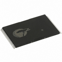
CY62167DV30LL-55ZXI Cypress Semiconductor Corp, CY62167DV30LL-55ZXI Datasheet - Page 5

CY62167DV30LL-55ZXI
Manufacturer Part Number
CY62167DV30LL-55ZXI
Description
IC SRAM 16MBIT 55NS 48TSOP
Manufacturer
Cypress Semiconductor Corp
Type
Asynchronousr
Datasheet
1.CY62167DV30LL-55ZXI.pdf
(17 pages)
Specifications of CY62167DV30LL-55ZXI
Memory Size
16M (1M x 16)
Package / Case
48-TSOP I
Format - Memory
RAM
Memory Type
SRAM
Speed
55ns
Interface
Parallel
Voltage - Supply
2.2 V ~ 3.6 V
Operating Temperature
-40°C ~ 85°C
Access Time
55 ns
Supply Voltage (max)
3.6 V
Supply Voltage (min)
2.2 V
Maximum Operating Current
30 mA
Maximum Operating Temperature
+ 85 C
Minimum Operating Temperature
- 40 C
Mounting Style
SMD/SMT
Number Of Ports
1
Operating Supply Voltage
2.5 V, 3.3 V
Lead Free Status / RoHS Status
Lead free / RoHS Compliant
Lead Free Status / RoHS Status
Lead free / RoHS Compliant, Lead free / RoHS Compliant
Other names
428-1860
Available stocks
Company
Part Number
Manufacturer
Quantity
Price
Company:
Part Number:
CY62167DV30LL-55ZXI
Manufacturer:
CYPRESS
Quantity:
1 200
Company:
Part Number:
CY62167DV30LL-55ZXIT
Manufacturer:
Cypress
Quantity:
28
Capacitance
Thermal Resistance
AC Test Loads and Waveforms
Data Retention Characteristics
Notes
Document Number : 38-05328 Rev. *I
C
C
V
I
t
t
Parameter
11. Tested initially and after any design or process changes that may affect these parameters.
12. Typical values are included for reference only and are not guaranteed or tested. Typical values are measured at V
13. Full device operation requires linear V
CCDR
CDR
R
Parameter
IN
OUT
DR
JA
JC
[13]
Parameter
[11]
OUTPUT
[11]
Parameters
V
Data retention current
Chip deselect to data retention time
Operation recovery time
CC
[11]
INCLUDING
V
Thermal resistance
(Junction to ambient)
Thermal resistance
(Junction to case)
R
V
R1
R2
for Data retention
CC
TH
JIG AND
TH
SCOPE
50 pF
Input capacitance
Output capacitance
[12]
Description
Description
Description
R1
CC
ramp from V
Equivalent to:
R2
(Over the Operating Range)
DR
16667
15385
2.5 V
OUTPUT
8000
to V
1.20
Still Air, soldered on a 3 × 4.5 inch,
2-layer printed circuit board
T
Rise Time = 1 V/ns
CC(min.)
A
= 25 °C, f = 1 MHz, V
> 100 s or stable at V
THE VENIN EQUIVALENT
CE
V
V
GND
V
CC
IN
Test Conditions
Test Conditions
CC
1
= 1.5 V,
> V
> V
CC
CC
10%
R
– 0.2 V or CE
– 0.2V or V
TH
CC
3.0 V
1554
1103
1.75
Conditions
645
CC(min.)
ALL INPUT PULSES
= V
90%
CY62167DV30LL-55
CY62167DV30LL-70
CC(typ)
V
IN
> 100 s.
2
< 0.2 V
< 0.2 V,
CC
VFBGA
CY62167DV30 MoBL
= V
90%
55
16
10%
CC(typ)
Max
10
Fall Time = 1 V/ns
8
Min
1.5
55
70
–
0
, T
A
= 25 °C
Unit
Typ
TSOP I
V
–
–
–
–
4.3
60
[12]
Max
10
Page 5 of 17
–
–
–
Unit
pF
pF
C / W
C / W
Unit
Unit
A
ns
ns
V


