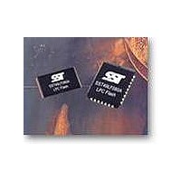
SST49LF080A-33-4C-WHE Microchip Technology, SST49LF080A-33-4C-WHE Datasheet - Page 11

SST49LF080A-33-4C-WHE
Manufacturer Part Number
SST49LF080A-33-4C-WHE
Description
IC FLASH SER LPC 8MBIT 32TSOP
Manufacturer
Microchip Technology
Datasheets
1.SST49LF080A-33-4C-NHE.pdf
(49 pages)
2.SST49LF080A-33-4C-NHE.pdf
(2 pages)
3.SST49LF080A-33-4C-NHE.pdf
(2 pages)
Specifications of SST49LF080A-33-4C-WHE
Memory Type
FLASH
Memory Size
8M (1M x 8)
Operating Temperature
0°C ~ 85°C
Package / Case
32-TSOP
Format - Memory
FLASH
Speed
33MHz
Interface
Parallel
Voltage - Supply
3 V ~ 3.6 V
Data Bus Width
8 bit
Architecture
Sectored
Interface Type
Parallel, Serial
Supply Voltage (max)
3.6 V
Supply Voltage (min)
3 V
Maximum Operating Current
12 mA
Mounting Style
SMD/SMT
Organization
4 KB x 256
Lead Free Status / RoHS Status
Lead free / RoHS Compliant
Lead Free Status / RoHS Status
Lead free / RoHS Compliant, Lead free / RoHS Compliant
Available stocks
Company
Part Number
Manufacturer
Quantity
Price
Company:
Part Number:
SST49LF080A-33-4C-WHE
Manufacturer:
SST
Quantity:
1 815
Part Number:
SST49LF080A-33-4C-WHE
Manufacturer:
SST
Quantity:
20 000
8 Mbit LPC Flash
SST49LF080A
CE#
The CE# pin, enables and disables the SST49LF080A,
controlling read and write access of the device. To enable
the SST49LF080A, the CE# pin must be driven low one
clock cycle prior to LFRAME# being driven low. The device
will enter standby mode when internal Write operations are
completed and CE# is high.
LFRAME#
The LFRAME# signifies the start of a (frame) bus cycle or
the termination of an undesired cycle. Asserting LFRAME#
for two or more clock cycle and driving a valid START value
on LAD[3:0] will initiate device operation. The device will
enter standby mode when internal operations are com-
pleted and LFRAME# is high.
TBL#, WP#
The Top Boot Lock (TBL#) and Write Protect (WP#) pins
are provided for hardware write protection of device mem-
ory. The TBL# pin is used to Write-Protect 16 boot sectors
(64 KByte) at the highest memory address range for the
SST49LF080A. The WP# pin write protects the remaining
sectors in the flash memory.
An active low signal at the TBL# pin prevents Program and
Erase operations of the top boot sectors. When TBL# pin is
held high, the write protection of the top boot sectors is dis-
abled. The WP# pin serves the same function for the
remaining sectors of the device memory. The TBL# and
WP# pins write protection functions operate independently
of one another.
TABLE 4: Address Decoding Range
©2006 Silicon Storage Technology, Inc.
1. For device #0 (Boot Device), SST49LF080A decodes the physical addresses of the top 2 blocks (including Boot Block) both at
Device #0 - 3
Device #4 - 7
Device #8 - 11
Device #12 - 15
Device #0
system memory ranges FFFF FFFFH to FFFE 0000H and 000F FFFFH to 000E 0000H.
ID Strapping
1
Memory Access
Register Access
Memory Access
Register Access
Memory Access
Register Access
Memory Access
Register Access
Memory Access
Device Access
11
FFFF FFFFH : FFC0 0000H
FFBF FFFFH : FF80 0000H
FE3F FFFFH : FE00 0000H
FF7F FFFFH : FF40 0000H
FF3F FFFFH : FF00 0000H
FEFF FFFFH : FEC0 0000H
FEBF FFFFH : FE80 0000H
FE7F FFFFH : FE40 0000H
000F FFFFH : 000E 0000H
Both TBL# and WP# pins must be set to their required pro-
tection states prior to starting a Program or Erase opera-
tion. A logic level change occurring at the TBL# or WP# pin
during a Program or Erase operation could cause unpre-
dictable results.
INIT#, RST#
A V
and RST# pins have the same function internally. It is
required to drive INIT# or RST# pins low during a system
reset to ensure proper CPU initialization. During a Read
operation, driving INIT# or RST# pins low deselects the
device and places the output drivers, LAD[3:0], in a high-
impedance state. The reset signal must be held low for a
minimal duration of time T
a reset procedure is performed during a Program or Erase
operation. See Table 17, Reset Timing Parameters for
more information. A device reset during an active Program
or Erase will abort the operation and memory contents may
become invalid due to data being altered or corrupted from
an incomplete Erase or Program operation.
System Memory Mapping
The LPC interface protocol has address length of 32-bit or
4 GByte. The SST49LF080A will respond to addresses in
the range as specified in Table 4.
Refer to “Multiple Device Selection” section for more detail
on strapping multiple SST49LF080A devices to increase
memory densities in a system and “Registers” section on
valid register addresses.
IL
Address Range
on INIT# or RST# pin initiates a device reset. INIT#
RSTP
. A reset latency will occur if
Memory Size
128 KByte
4 MByte
4 MByte
4 MByte
4 MByte
4 MByte
4 MByte
4 MByte
4 MByte
S71235-02-000
Data Sheet
T4.0 1235
5/06


