CY7C199CNL-15VXI Cypress Semiconductor Corp, CY7C199CNL-15VXI Datasheet
CY7C199CNL-15VXI
Specifications of CY7C199CNL-15VXI
Available stocks


Related parts for CY7C199CNL-15VXI


CY7C199CNL-15VXI Summary of contents
Page 1
... Logic Block Diagram Product Portfolio Maximum Access Time Maximum Operating Current Maximum CMOS Standby Current (low power) Cypress Semiconductor Corporation Document #: 001-06435 Rev. *E 256 K (32 K × 8) Static RAM General Description The CY7C199CN is a high performance CMOS Asynchronous SRAM organized as 32K by 8 bits that supports an asynchronous memory interface ...
Page 2
Contents Pin Layout and Specifications ........................................ 3 Pin Description ................................................................. 4 Truth Table ........................................................................ 4 Maximum Ratings ............................................................. 4 Operating Range ............................................................... 4 ........................................................................................ 5 Capacitance ........................................................................ 5 Thermal Resistance DC Electrical Characteristics .......................................... 5 AC Test Loads .................................................................. 6 ...
Page 3
Pin Layout and Specifications 28 DIP ...
Page 4
Pin Description Pin Type Description A Input Address Inputs X CE Control Chip Enable IO Input or Output Data Input Outputs X OE Control Output Enable V Supply Power (5.0V Supply Ground SS WE Control Write Enable Truth ...
Page 5
DC Electrical Characteristics [2] Over the Operating Range (–15, –20) Parameter Description V Input HIGH Voltage IH V Input LOW Voltage IL V Output HIGH Voltage Output LOW Voltage Operating Supply V CC ...
Page 6
AC Test Loads ...
Page 7
... HZWE 7. The internal memory write time is defined by the overlap of CE LOW and WE LOW. CE and WE must be LOW to initiate a write, and the transition of any of these signals can terminate the write. The input data setup and hold timing must be referenced to the leading edge of the signal that terminates the write. ...
Page 8
Timing Waveforms Data Retention Waveform CDR CE [9, 10] Read Cycle 1 Address Data Out Previous Data Valid Document #: 001-06435 Rev. *E DATA RETENTION MODE OHA CY7C199CN t R Data Valid ...
Page 9
Timing Waveforms (continued) [11, 12] Read Cycle 2 Address CE OE High Z Data Out Current Notes 9. Device is continuously selected CE HIGH for read ...
Page 10
Timing Waveforms (continued) [13, 14, 15] Write Cycle 1 (WE controlled) Address HZOE Undefined Data In/Out see footnotes Document #: 001-06435 Rev SCE PWE ...
Page 11
Timing Waveforms (continued) [14, 16, 17] Write Cycle 2 (CE controlled) Address CE WE High Z Data In/Out Notes 13. This cycle is WE controlled HIGH during write. 14. Data in and/or out is high impedance if OE ...
Page 12
Timing Waveforms (continued) Write Cycle 3 (WE controlled, OE low) Address Data Undefined In Out see footnotes Note 18. The cycle is WE controlled, OE LOW. The minimum write cycle time is the sum of t ...
Page 13
... Ordering Information Contact local sales representative regarding availability of these parts. Speed Package Ordering Code (ns) Diagram 15 CY7C199CN-15PXC 51-85014 CY7C199CN-15VXC 51-85031 CY7C199CNL-15VXI 51-85031 20 CY7C199CN-20ZXI 51-85071 Ordering Code Definitions Document #: 001-06435 Rev. *E Package Type 28 DIP (6.9 x 35.6 x 3.5 mm), Pb-free 28-Pin (300-Mil) Molded SOJ, Pb-free 28-Pin (300-Mil) Molded SOJ, Pb-free 28 TSOP ...
Page 14
Package Diagrams Figure 1. 28-pin TSOP 13.4 mm), 51-85071 Document #: 001-06435 Rev. *E CY7C199CN 51-85071 *I Page [+] Feedback ...
Page 15
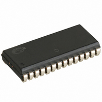
Package Diagrams (continued) Figure 2. 28-pin (300 Mil) Molded SOJ, 51-85031 Document #: 001-06435 Rev. *E CY7C199CN 51-85031 *D Page [+] Feedback ...
Page 16
Package Diagrams (continued) Document #: 001-06435 Rev. *E Figure 3. 28-pin (300 Mil) PDIP, 51-85014 CY7C199CN 51-85014 *E Page [+] Feedback ...
Page 17
... Acronym Description CE chip enable CMOS Complementary metal oxide semiconductor I/O Input/output OE output enable SRAM Static random access memory SOJ Small Outline J-Lead TSOP Thin Small Outline Package VFBGA Very Fine-Pitch Ball Grid Array Document #: 001-06435 Rev. *E Document Conventions Units of Measure Symbol ...
Page 18
... Cypress against all charges. Any Source Code (software and/or firmware) is owned by Cypress Semiconductor Corporation (Cypress) and is protected by and subject to worldwide patent protection (United States and foreign), United States copyright laws and international treaty provisions. Cypress hereby grants to licensee a personal, non-exclusive, non-transferable license to copy, use, modify, create derivative works of, and compile the Cypress Source Code and derivative works for the sole purpose of creating custom software and or firmware in support of licensee product to be used only in conjunction with a Cypress integrated circuit as specified in the applicable agreement ...