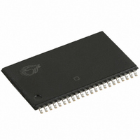
CY62136ESL-45ZSXI Cypress Semiconductor Corp, CY62136ESL-45ZSXI Datasheet

CY62136ESL-45ZSXI
Specifications of CY62136ESL-45ZSXI
Related parts for CY62136ESL-45ZSXI
CY62136ESL-45ZSXI Summary of contents
Page 1
... Available in Pb-free 44-pin thin small outline package (TSOP) II ■ package Functional Description The CY62136ESL is a high performance CMOS static RAM organized as 128K words by 16 bits. This device features advanced circuit design to provide ultra low active current. This is ideal for providing More Battery Life (MoBL ...
Page 2
... Operating Range ................................................................. 4 Electrical Characteristics ................................................... 4 Thermal Resistance ............................................................ 5 Capacitance. ....................................................................... 5 Data Retention Characteristics ......................................... 6 Data Retention Waveform .................................................. 6 Switching Characteristics .................................................. 7 Switching Waveforms ........................................................ 8 Document #: 001-48147 Rev. *C CY62136ESL MoBL Truth Table ........................................................................ 11 Ordering Information ....................................................... 12 Ordering Code Definition ............................................. 12 Package Diagram ............................................................. 13 Acronyms .......................................................................... 13 Document Conventions ................................................... 13 Units of Measure ......................................................... 13 Document History Page ................................................... 14 Sales, Solutions, and Legal Information ........................ 15 Worldwide Sales and Design Support ...
Page 3
... BLE I I I/O I I/O I I/O I Speed Range (V) [2] CC (ns 1MHz Typ the range CY62136ESL MoBL [1] Power Dissipation Operating I , (mA) CC Standby, I ( max [3] Max Typ [3] Max Typ [3] 2 3V, and ° Page SB2 Max 7 [+] Feedback ...
Page 4
... V CC CC(max) – 0 > V – 0 < 0 CC(max) CC (min) and 200 s wait time after SB1 CY62136ESL MoBL [4, 5] ........................................–0 6.0 V Ambient Range V CC Temperature Industrial –40 ° 5°C 2.2 V–3.6 V, and 4.5 V–5 Min Typ [7] Max 2.0 – – ...
Page 5
... Figure 2. AC Test Loads and Waveforms ALL INPUT PULSES V CC 90% 10% GND Rise Time = 1 V/ns R2 Equivalent to: THÉ VENIN EQUIVALENT OUTPUT 3.0 V 1103 1554 645 1.75 CY62136ESL MoBL Max Unit TSOP II Unit 90% 10% Fall Time = 1 V/ ...
Page 6
... V – 0 < 0 Figure 3. Data Retention Waveform DATA RETENTION MODE V V > 1.0 V CC(min CDR / I SB1 SB2 > 100 s or stable at V > 100 CC(min) CC(min) CY62136ESL MoBL Min Typ [10] Max 1.0 – – = 1.0 V – 0 – – 45 – – V CC(min specification. Other inputs can be left floating ...
Page 7
... The data input setup and hold timing must be referenced to the edge of the signal that terminates the write. Document #: 001-48147 Rev. *C Description [16] [16, 17] as shown in the AC Test Loads and Waveforms on page 5 is less than less than less than t LZCE HZBE LZBE HZOE , BHE, BLE or both = V IL CY62136ESL MoBL 45 ns Unit Min Max 45 – ns – – ns – – ...
Page 8
... The device is continuously selected HIGH for read cycle. 21. Address valid before or similar to CE, BHE, BLE transition LOW. Document #: 001-48147 Rev OHA DOE t DBE DATA VALID 50% , BHE, BLE, or both = CY62136ESL MoBL [19, 20] DATA VALID [20, 21 HZCE t HZOE t HZBE HIGH IMPEDANCE Page [+] Feedback ...
Page 9
... IH 25. During this period, the I/Os are in output state. Do not apply input signals. Document #: 001-48147 Rev SCE PWE DATA IN Figure 7. Write Cycle 2: CE Controlled SCE PWE DATA IN CY62136ESL MoBL [22, 23, 24 [22, 23, 24 Page [+] Feedback ...
Page 10
... If CE goes HIGH simultaneously with WE = VIH, the output remains in a high impedance state. 27. During this period, the I/Os are in output state. Do not apply input signals. Document #: 001-48147 Rev SCE PWE t SD DATA IN t HZWE SCE PWE t HZWE t SD DATA IN CY62136ESL MoBL [26 LZWE [26 LZWE Page [+] Feedback ...
Page 11
... Output disabled H High-Z Output disabled L Data in (I/O –I/O ) Write Data in (I/O –I/O ); Write 0 7 I/O –I/O in High Data in (I/O –I/O ); Write 8 15 I/O –I/O in High CY62136ESL MoBL Mode Power Standby ( Active ( Active ( Active ( Active ( Active ( Active ( Active ( Active ( Active ( Active ( ...
Page 12
... Ordering Information Speed Ordering Code (ns) 45 CY62136ESL-45ZSXI Ordering Code Definition CY 621 ZSX Document #: 001-48147 Rev. *C Package Package Type Diagram 51-85087 44-Pin TSOP Type II (Pb-free) I Temperature Grades I = Industrial ZSX = TSOP Type II (Pb-free) Speed Grade Wide Voltage Range (3 V and Process Technology 90 nm ...
Page 13
... BASE PLANE 0.10 (.004) 0°-5° SEATING PLANE Document Conventions Units of Measure Symbol °C A mA MHz W CY62136ESL MoBL EJECTOR MARK (OPTIONAL) CAN BE LOCATED BOTTOM VIEW ANYWHERE IN THE BOTTOM PKG 10.262 (0.404) 10.058 (0.396) 0.210 (0.0083) 0.120 (0.0047) 0.597 (0.0235) ...
Page 14
... Document History Page Document Title: CY62136ESL MoBL Document Number: 001-48147 Orig. of Rev. ECN No. Change ** 2615537 VKN/PYRS *A 2718906 VKN *B 2944332 VKN *C 3126445 RAME Document #: 001-48147 Rev Mbit (128K x 16) Static RAM Submission Date Description of Change 12/03/08 New Data Sheet 06/15/2009 Post to external web ...
Page 15
... Use may be limited by and subject to the applicable Cypress software license agreement. Document #: 001-48147 Rev. *C MoBL is a registered trademark and More Battery Life is a trademark of Cypress Semiconductor. All product and company names mentioned in this document are the trademarks of their respective holders. cypress.com/go/plc Revised January 03, 2011 CY62136ESL MoBL PSoC Solutions psoc.cypress.com/solutions PSoC 1 | ...


