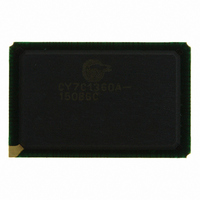
CY7C1360A-150BGC Cypress Semiconductor Corp, CY7C1360A-150BGC Datasheet - Page 20

CY7C1360A-150BGC
Manufacturer Part Number
CY7C1360A-150BGC
Description
IC SRAM 9MBIT 150MHZ 119BGA
Manufacturer
Cypress Semiconductor Corp
Datasheet
1.CY7C1360A-150BGC.pdf
(28 pages)
Specifications of CY7C1360A-150BGC
Format - Memory
RAM
Memory Type
SRAM - Synchronous
Memory Size
9M (256K x 36)
Speed
150MHz
Interface
Parallel
Voltage - Supply
3.135 V ~ 3.6 V
Operating Temperature
0°C ~ 70°C
Package / Case
119-BGA
Lead Free Status / RoHS Status
Contains lead / RoHS non-compliant
Other names
428-1115
Available stocks
Company
Part Number
Manufacturer
Quantity
Price
Company:
Part Number:
CY7C1360A-150BGC
Manufacturer:
Cypress Semiconductor Corp
Quantity:
10 000
Document #: 38-05258 Rev. *C
Thermal Resistance
AC Test Loads and Waveforms
OUTPUT
Switching Characteristics
Clock
t
t
t
Output Times
t
t
t
t
t
t
t
Set-up Times
t
Hold Times
t
Notes:
26. Typical values are measured at 3.3V, 25°C, and 20 ns cycle time.
27. Test conditions as specified with the output loading as shown in part (a) of AC Test Loads unless otherwise noted.
28. At any given temperature and voltage condition, t
29. OE is a “Don’t Care” when a byte Write enable is sampled LOW.
30. This is a synchronous device. All synchronous inputs must meet specified set up and hold time, except for “Don’t Care” as defined in the truth table.
Parameter
KC
KH
KL
KQ
KQX
KQLZ
KQHZ
OEQ
OELZ
OEHZ
S
H
Parameter
JA
JC
(a)
Z
0
= 50
Clock Cycle Time
Clock HIGH Time
Clock LOW Time
Clock to Output Valid
Clock to Output Invalid
Clock to Output in Low-Z
Clock to Output in High-Z
OE to Output Valid
OE to Output in Low-Z
OE to Output in High-Z
Address, Controls, and Data In
Address, Controls, and Data In
Thermal Resistance (Junction to Ambient) Still Air, soldered on a 4.25 x 1.125 inch,
Thermal Resistance (Junction to Case)
V
TH
= 1.5V
R
L
= 50
[15]
OUTPUT
Description
Description
[29]
INCLUDING
V
CCQ
Over the Operating Range
JIG AND
SCOPE
(b)
[15, 22, 28]
[15, 22, 28]
[15, 22, 28]
5 pF
[15, 22, 28]
KQHZ
V
V
V
V
[30]
[30]
CCQ
CCQ
CCQ
CCQ
R = 317
is less than t
= 3.3V
= 2.5V
= 3.3V
= 2.5V
R = 351
KQLZ
4-layer PCB
Min.
1.25
1.25
4.4
1.8
1.8
1.4
0.4
[27]
GND
V
and t
225 MHz
0
0
CCQ
1 V/ns
OEHZ
10%
Max.
2.8
2.8
3.0
2.8
2.8
2.8
is less than t
ALL INPUT PULSES
Test Conditions
90%
(c)
Min.
1.25
1.25
5.0
2.0
2.0
1.4
0.4
200 MHz
0
0
OELZ
Max.
.
3.1
3.1
2.6
3.0
3.0
3.0
90%
10%
1 V/ns
Min.
1.25
6.0
2.4
2.4
1.0
1.5
0.5
166 MHz
0
0
Vccmin
Vcctyp
Max.
t
3.5
4.0
2.8
3.5
4.0
3.5
PU = 200us
TQFP Typ.
Min.
1.25
1.25
6.7
2.6
2.6
2.0
0.5
CY7C1360A
CY7C1362A
150 MHz
0
0
25
9
(d)
Page 20 of 28
Max.
For proper RESET
bring Vcc down to 0V
3.5
4.5
4.0
3.5
4.5
3.5
Unit
Unit
C/W
C/W
ns
ns
ns
ns
ns
ns
ns
ns
ns
ns
ns
ns
ns
ns


