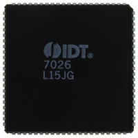
IDT7026L15JG IDT, Integrated Device Technology Inc, IDT7026L15JG Datasheet - Page 10

IDT7026L15JG
Manufacturer Part Number
IDT7026L15JG
Description
IC SRAM 256KBIT 15NS 84PLCC
Manufacturer
IDT, Integrated Device Technology Inc
Datasheet
1.IDT7026L15JG.pdf
(18 pages)
Specifications of IDT7026L15JG
Format - Memory
RAM
Memory Type
SRAM - Dual Port, Asynchronous
Memory Size
256K (16K x 16)
Speed
15ns
Interface
Parallel
Voltage - Supply
4.5 V ~ 5.5 V
Operating Temperature
0°C ~ 70°C
Package / Case
84-PLCC
Lead Free Status / RoHS Status
Lead free / RoHS Compliant
Other names
7026L15JG
800-1366
800-1366-5
800-1366
800-1366
800-1366-5
800-1366
Available stocks
Company
Part Number
Manufacturer
Quantity
Price
Company:
Part Number:
IDT7026L15JG
Manufacturer:
IDT Integrated Device Technolo
Quantity:
135
Company:
Part Number:
IDT7026L15JG
Manufacturer:
IDT, Integrated Device Technology Inc
Quantity:
10 000
Timing Waveform of Write Cycle No. 1, R/W Controlled Timing
Timing Waveform of Write Cycle No. 2, CE, UB, LB Controlled Timing
NOTES:
1. R/W or CE or UB and LB = V
2. A write occurs during the overlap (t
3. t
4. During this period, the I/O pins are in the output state and input signals must not be applied.
5. If the CE or SEM = V
6. Timing depends on which enable signal is asserted last, CE or R/W.
7. This parameter is guaranteed by device characterization, but is not production tested. Transition is measured 0mV from steady state with the Output Test Load (Figure
8. If OE = V
9. To access RAM, CE = V
CE or SEM
CE or SEM
ADDRESS
ADDRESS
IDT7026S/L
High-Speed 16K x 16 Dual-Port Static RAM
DATA
2).
on the bus for the required t
specified t
UB or LB
UB or LB
WR
DATA
DATA
is measured from the earlier of CE or R/W (or SEM or R/W) going V
R/W
R/W
OUT
OE
IN
IL
IN
WP
during R/W controlled write cycle, the write pulse width must be the larger of t
(9)
(9)
(9)
(9)
.
IL
transition occurs simultaneously with or after the R/W = V
IL
and SEM = V
DW
IH
. If OE = V
t
during all address transitions.
AS
t
AS
EW
(6)
(6)
or t
IH
WP
(4)
. To access semaphore, CE = V
IH
) of a V
during an R/W controlled write cycle, this requirement does not apply and the write pulse can be as short as the
IL
CE = V
t
WZ
(7)
t
t
AW
AW
IL
t
WC
t
and R/W = V
WC
t
t
WP
EW
IH
(2)
(2)
IH
to the end of write cycle.
6.42
10
and SEM = V
IL
for memory array writing cycle.
IL
transition, the outputs remain in the High-impedance state.
t
t
DW
DW
WP
Military, Industrial and Commercial Temperature Ranges
IL
or (t
. t
EW
WZ
must be met for either condition.
+ t
t
WR
DW
(3)
) to allow the I/O drivers to turn off and data to be placed
t
t
t
DH
DH
WR
t
OW
(3)
t
HZ
(7)
(4)
(1,5,8)
2939 drw 09
2939 drw 08
(1,5)


