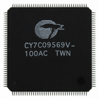
CY7C09569V-100AC Cypress Semiconductor Corp, CY7C09569V-100AC Datasheet - Page 5

CY7C09569V-100AC
Manufacturer Part Number
CY7C09569V-100AC
Description
IC SRAM 576KBIT 100MHZ 144LQFP
Manufacturer
Cypress Semiconductor Corp
Specifications of CY7C09569V-100AC
Format - Memory
RAM
Memory Type
SRAM - Dual Port, Synchronous
Memory Size
576K (16K x 36)
Speed
100MHz
Interface
Parallel
Voltage - Supply
3 V ~ 3.6 V
Operating Temperature
0°C ~ 70°C
Package / Case
144-LQFP
Density
576Kb
Access Time (max)
12.5ns
Sync/async
Synchronous
Architecture
SDR
Clock Freq (max)
67MHz
Operating Supply Voltage (typ)
3.3V
Address Bus
14b
Package Type
TQFP
Operating Temp Range
0C to 70C
Number Of Ports
2
Supply Current
385mA
Operating Supply Voltage (min)
3.135V
Operating Supply Voltage (max)
3.465V
Operating Temperature Classification
Commercial
Mounting
Surface Mount
Pin Count
144
Word Size
36b
Number Of Words
16K
Lead Free Status / RoHS Status
Contains lead / RoHS non-compliant
Other names
428-1189
Available stocks
Company
Part Number
Manufacturer
Quantity
Price
Company:
Part Number:
CY7C09569V-100AC
Manufacturer:
Cypress Semiconductor Corp
Quantity:
10 000
Part Number:
CY7C09569V-100AC
Manufacturer:
CYP
Quantity:
20 000
Selection Guide
Pin Definitions
Document #: 38-06054 Rev. *A
f
Max. Access Time (ns) (Clock to Data, Pipelined)
Typical Operating Current I
Typical Standby Current for I
Typical Standby Current for I
A
ADS
CE
CLK
CNTEN
CNTRST
I/O
OE
R/W
FT/PIPE
B
V
V
MAX2
0L
0L
SS
DD
Left Port
0L
L
L
–A
–B
L
L
L
–I/O
(MHz) (Pipelined)
13/14L
3L
L
L
L
35L
A
ADS
CE
CLK
CNTEN
CNTRST
I/O
OE
R/W
FT/PIPE
BM, SIZE
BE
Right Port
0R
0R
R
R
–A
R
R
R
–I/O
13/14R
R
R
R
35R
CC
SB3
SB1
(mA)
( A) (Both Ports CMOS Level)
Address Inputs (A
Address Strobe Input. Used as an address qualifier. This signal should be asserted LOW to
assert the part using the externally supplied address on Address Pins. To load this address into
the Burst Address Counter both ADS and CNTEN have to be LOW. ADS is disabled if CNTRST
is asserted LOW
Chip Enable Input.
Clock Signal. This input can be free-running or strobed. Maximum clock input rate is f
Counter Enable Input. Asserting this signal LOW increments the burst address counter of its
respective port on each rising edge of CLK. CNTEN is disabled if CNTRST is asserted LOW.
Counter Reset Input. Asserting this signal LOW resets the burst address counter of its respec-
tive port to zero. CNTRST is not disabled by asserting ADS or CNTEN.
Data Bus Input/Output.
Output Enable Input. This signal must be asserted LOW to enable the I/O data pins during read
operations.
Read/Write Enable Input. This signal is asserted LOW to write to the dual port memory array.
For read operations, assert this pin HIGH.
Flow-Through/Pipelined Select Input. For flow-through mode operation, assert this pin LOW.
For pipelined mode operation, assert this pin HIGH.
Byte Select Inputs. Asserting these signals enable read and write operations to the correspond-
ing bytes of the memory array.
Select Pins for Bus Matching. See Bus Matching for details.
Big Endian Pin. See Bus Matching for details.
Ground Input.
Power Input.
(mA) (Both Ports TTL Level)
0
–A
13
for 16K, A
CY7C09569V
CY7C09579V
0
–A
14
10 A
-100
100
250
30
Description
for 32K devices).
5
CY7C09569V
CY7C09579V
10 A
240
-83
83
25
6
CY7C09569V
CY7C09579V
CY7C09569V
CY7C09579V
10 A
Page 5 of 30
230
-67
67
25
8
MAX
.


