CAT24C32WI-G ON Semiconductor, CAT24C32WI-G Datasheet - Page 6
CAT24C32WI-G
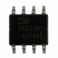
Manufacturer Part Number
CAT24C32WI-G
Description
IC EEPROM 32KBIT 400KHZ 8SOIC
Manufacturer
ON Semiconductor
Datasheet
1.CAT24C32YI-GT3.pdf
(16 pages)
Specifications of CAT24C32WI-G
Format - Memory
EEPROMs - Serial
Memory Type
EEPROM
Memory Size
32K (4K x 8)
Speed
400kHz
Interface
I²C, 2-Wire Serial
Voltage - Supply
1.8 V ~ 5.5 V
Operating Temperature
-40°C ~ 85°C
Package / Case
8-SOIC (3.9mm Width)
Organization
128 K Pages x 256
Interface Type
I2C
Maximum Clock Frequency
0.1 MHz
Access Time
3500 ns
Supply Voltage (max)
5.5 V
Supply Voltage (min)
1.7 V
Maximum Operating Current
2 mA
Maximum Operating Temperature
+ 85 C
Mounting Style
SMD/SMT
Minimum Operating Temperature
- 40 C
Operating Supply Voltage
1.8 V , 2.5 V , 3.3 V , 5 V
Lead Free Status / RoHS Status
Lead free / RoHS Compliant
Available stocks
Company
Part Number
Manufacturer
Quantity
Price

Part Number:
CAT24C32WI-G
Manufacturer:
ON/安森美
Quantity:
20 000
Company:
Part Number:
CAT24C32WI-GT3
Manufacturer:
CATALYST
Quantity:
3 515
Part Number:
CAT24C32WI-GT3
Manufacturer:
ON/安森美
Quantity:
20 000
Company:
Part Number:
CAT24C32WI-GT3JN
Manufacturer:
ON Semiconductor
Quantity:
2 200


Byte Write
condition on the bus and then broadcasts a Slave address
with the R/W bit set to ‘0’. The Master then sends two
address bytes and a data byte and concludes the session by
creating a STOP condition on the bus. The Slave responds
with ACK after every byte sent by the Master (Figure 6). The
STOP starts the internal Write cycle, and while this
operation is in progress (t
and the Slave does not acknowledge the Master (Figure 7).
Page Write
by sending more than one data byte to the Slave before
issuing the STOP condition (Figure 8). Up to 32 distinct data
bytes can be loaded into the internal Page Write Buffer
starting at the address provided by the Master. The page
address is latched, and as long as the Master keeps sending
data, the internal byte address is incremented up to the end
of page, where it then wraps around (within the page). New
data can therefore replace data loaded earlier. Following the
STOP, data loaded during the Page Write session will be
written to memory in a single internal Write cycle (t
To write data to memory, the Master creates a START
The Byte Write operation can be expanded to Page Write,
FROM TRANSMITTER
SDA OUT
FROM RECEIVER
SDA IN
SCL
DATA OUTPUT
DATA OUTPUT
SCL FROM
MASTER
t
SU:STA
START
WR
), the SDA output is tri-stated
t
BUS RELEASE DELAY (TRANSMITTER)
F
t
HD:SDA
t
LOW
1
t
Figure 4. Acknowledge Timing
AA
t
HD:DAT
ACK DELAY (≤ t
t
WRITE OPERATIONS
HIGH
Figure 5. Bus Timing
http://onsemi.com
WR
).
t
LOW
6
AA
Acknowledge Polling
Slave will not acknowledge the Master. This feature enables
the Master to immediately follow-up with a new Read or
Write request, rather than wait for the maximum specified
Write time (t
response from the Slave, the Master simply repeats the
request until the Slave responds with ACK.
Hardware Write Protection
protected against Write operations. If the WP pin is left
floating or is grounded, it has no impact on the Write
operation. The state of the WP pin is strobed on the last
falling edge of SCL immediately preceding the 1
(Figure 9). If the WP pin is HIGH during the strobe interval,
the Slave will not acknowledge the data byte and the Write
request will be rejected.
Delivery State
)
8
t
DH
As soon (and as long) as internal Write is in progress, the
With the WP pin held HIGH, the entire memory is
The CAT24C32 is shipped erased, i.e., all bytes are FFh.
t
SU:DAT
t
R
WR
9
ACK SETUP (≥ t
) to elapse. Upon receiving a NoACK
BUS RELEASE DELAY (RECEIVER)
SU:DAT
t
t
BUF
SU:STO
)
st
data byte
Related parts for CAT24C32WI-G
Image
Part Number
Description
Manufacturer
Datasheet
Request
R

Part Number:
Description:
ON Semiconductor [VOLTAGE REGULATOR]
Manufacturer:
ON Semiconductor
Datasheet:
Part Number:
Description:
357-036-542-201 CARDEDGE 36POS DL .156 BLK LOPRO
Manufacturer:
ON Semiconductor
Datasheet:
Part Number:
Description:
357-036-542-201 CARDEDGE 36POS DL .156 BLK LOPRO
Manufacturer:
ON Semiconductor
Datasheet:
Part Number:
Description:
357-036-542-201 CARDEDGE 36POS DL .156 BLK LOPRO
Manufacturer:
ON Semiconductor
Datasheet:
Part Number:
Description:
357-036-542-201 CARDEDGE 36POS DL .156 BLK LOPRO
Manufacturer:
ON Semiconductor
Datasheet:
Part Number:
Description:
357-036-542-201 CARDEDGE 36POS DL .156 BLK LOPRO
Manufacturer:
ON Semiconductor
Datasheet:
Part Number:
Description:
357-036-542-201 CARDEDGE 36POS DL .156 BLK LOPRO
Manufacturer:
ON Semiconductor
Datasheet:
Part Number:
Description:
357-036-542-201 CARDEDGE 36POS DL .156 BLK LOPRO
Manufacturer:
ON Semiconductor
Datasheet:
Part Number:
Description:
357-036-542-201 CARDEDGE 36POS DL .156 BLK LOPRO
Manufacturer:
ON Semiconductor
Datasheet:
Part Number:
Description:
357-036-542-201 CARDEDGE 36POS DL .156 BLK LOPRO
Manufacturer:
ON Semiconductor
Datasheet:
Part Number:
Description:
357-036-542-201 CARDEDGE 36POS DL .156 BLK LOPRO
Manufacturer:
ON Semiconductor
Datasheet:
Part Number:
Description:
Manufacturer:
ON Semiconductor
Datasheet:
Part Number:
Description:
Manufacturer:
ON Semiconductor
Datasheet:
Part Number:
Description:
Manufacturer:
ON Semiconductor
Datasheet: