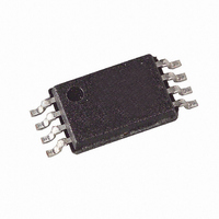
AT25128B-XHL-B Atmel, AT25128B-XHL-B Datasheet - Page 5

AT25128B-XHL-B
Manufacturer Part Number
AT25128B-XHL-B
Description
IC EEPROM 128KBIT 20MHZ 8TSSOP
Manufacturer
Atmel
Datasheet
1.AT25128B-SSHL-B.pdf
(24 pages)
Specifications of AT25128B-XHL-B
Format - Memory
EEPROMs - Serial
Memory Type
EEPROM
Memory Size
128K (16K x 8)
Speed
5MHz, 10MHz, 20MHz
Interface
SPI, 3-Wire Serial
Voltage - Supply
1.8 V ~ 5.5 V
Operating Temperature
-40°C ~ 85°C
Package / Case
8-TSSOP
Density
128Kb
Interface Type
Serial (SPI)
Organization
16Kx8
Access Time (max)
80ns
Frequency (max)
5MHz
Write Protection
Yes
Data Retention
100Year
Operating Supply Voltage (typ)
2.5/3.3/5V
Operating Temp Range
-40C to 85C
Supply Current
10mA
Operating Supply Voltage (min)
1.8V
Operating Supply Voltage (max)
5.5V
Operating Temperature Classification
Industrial
Mounting
Surface Mount
Pin Count
8
Lead Free Status / RoHS Status
Lead free / RoHS Compliant
Available stocks
Company
Part Number
Manufacturer
Quantity
Price
Part Number:
AT25128B-XHL-B
Manufacturer:
ATMEL/爱特梅尔
Quantity:
20 000
8698B–SEEPR–3/10
2.
Table 1-3.
Applicable over recommended operating range from T
CL = 1 TTL Gate and 30 pF (unless otherwise noted)
Notes:
Serial Interface Description
MASTER: The device that generates the serial clock.
SLAVE: Because the serial clock pin (SCK) is always an input, the AT25128B/256B always operates as a slave.
TRANSMITTER/RECEIVER: The AT25128B/256B has separate pins designated for data transmission (SO) and
reception (SI).
MSB: The Most Significant Bit (MSB) is the first bit transmitted and received.
SERIAL-OP CODE: After the device is selected with CS going low, the first byte will be received. This byte con-
tains the op-code that defines the operations to be performed.
INVALID OP-CODE: If an invalid op-code is received, no data will be shifted into the AT25128B/256B, and the
serial output pin (SO) will remain in a high impedance state until the falling edge of CS is detected again. This will
reinitialize the serial communication.
CHIP SELECT: The AT25128B/256B is selected when the CS pin is low. When the device is not selected, data will
not be accepted via the SI pin, and the serial output pin (SO) will remain in a high impedance state.
HOLD: The HOLD pin is used in conjunction with the CS pin to select the AT25128B/256B. When the device is
selected and a serial sequence is underway, HOLD can be used to pause the serial communication with the mas-
ter device without resetting the serial sequence. To pause, the HOLD pin must be brought low while the SCK pin is
low. To resume serial communication, the HOLD pin is brought high while the SCK pin is low (SCK may still toggle
during HOLD). Inputs to the SI pin will be ignored while the SO pin is in the high impedance state.
WRITE PROTECT: The write protect pin (WP) will allow normal read/write operations when held high. When the
WP pin is brought low and WPEN bit is “1”, all write operations to the status register are inhibited. WP going low
while CS is still low will interrupt a write to the status register. If the internal write cycle has already been initiated,
WP going low will have no effect on any write operation to the status register. The WP pin function is blocked when
the WPEN bit in the status register is “0”. This will allow the user to install the AT25128B/256B in a system with the
WP pin tied to ground and still be able to write to the status register. All WP pin functions are enabled when the
WPEN bit is set to “1”.
Symbol
t
t
t
t
Endurance
(1)
HZ
DIS
WC
LZ
1. This parameter is characterized and is not 100% tested. Contact Atmel for further information.
Parameter
HOLD to Output Low Z
HOLD to Output High Z
Output Disable Time
Write Cycle Time
3.3V, 25°C, Page Mode
AC Characteristics (Continued)
Voltage
4.5–5.5
2.5–5.5
1.8–5.5
4.5–5.5
2.5–5.5
1.8–5.5
4.5–5.5
2.5–5.5
1.8–5.5
4.5–5.5
2.5–5.5
1.8–5.5
A
=
–
40°C to + 85°C, V
Min
1M
0
0
0
CC
= As Specified,
AT25128B/256B
Max
100
100
100
25
50
25
50
25
50
5
5
5
Write Cycles
Units
ms
ns
ns
ns
5


