AT25DF641-MWH-T Atmel, AT25DF641-MWH-T Datasheet - Page 3
AT25DF641-MWH-T
Manufacturer Part Number
AT25DF641-MWH-T
Description
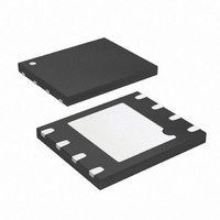
IC FLASH 64MBIT 100MHZ 8VDFN
Manufacturer
Atmel
Datasheet
1.AT25DF641-MWH-T.pdf
(56 pages)
Specifications of AT25DF641-MWH-T
Format - Memory
FLASH
Memory Type
DataFLASH
Memory Size
64M (32K pages x 256 bytes)
Speed
100MHz
Interface
SPI, 3-Wire Serial
Voltage - Supply
2.7 V ~ 3.6 V
Operating Temperature
-40°C ~ 85°C
Package / Case
8-VDFN
Lead Free Status / RoHS Status
Lead free / RoHS Compliant
Available stocks
Company
Part Number
Manufacturer
Quantity
Price
Company:

Part Number:
AT25DF641-MWH-T
Manufacturer:
XILINX
Quantity:
210
Part Number:
AT25DF641-MWH-T
Manufacturer:
ATMEL/爱特梅尔
Quantity:
20 000


1.
3680F–DFLASH–4/10
Pin Descriptions and Pinouts
Table 1-1.
SCK
SI (SIO)
SO (SOI)
CS
WP
Symbol
Name and Function
CHIP SELECT: Asserting the
deasserted, the device will be deselected and normally be placed in standby
mode (not Deep Power-Down mode), and the SO pin will be in a high-impedance
state. When the device is deselected, data will not be accepted on the SI pin.
A high-to-low transition on the
to-high transition is required to end an operation. When ending an internally self-
timed operation such as a program or erase cycle, the device will not enter the
standby mode until the completion of the operation.
SERIAL CLOCK: This pin is used to provide a clock to the device and is used to
control the flow of data to and from the device. Command, address, and input
data present on the SI pin is always latched in on the rising edge of SCK, while
output data on the SO pin is always clocked out on the falling edge of SCK.
SERIAL INPUT (SERIAL INPUT/OUTPUT): The SI pin is used to shift data into
the device. The SI pin is used for all data input including command and address
sequences. Data on the SI pin is always latched in on the rising edge of SCK.
With the Dual-Output Read Array command, the SI pin becomes an output pin
(SIO) to allow two bits of data (on the SO and SIO pins) to be clocked out on
every falling edge of SCK. To maintain consistency with SPI nomenclature, the
SIO pin will be referenced as SI throughout the document with exception to
sections dealing with the Dual-Output Read Array command in which it will be
referenced as SIO.
Data present on the SI pin will be ignored whenever the device is deselected
(
SERIAL OUTPUT (SERIAL OUTPUT/INPUT): The SO pin is used to shift data
out from the device. Data on the SO pin is always clocked out on the falling edge
of SCK.
With the Dual-Input Byte/Page Program command, the SO pin becomes an input
pin (SOI) to allow two bits of data (on the SOI and SI pins) to be clocked in on
every rising edge of SCK. To maintain consistency with SPI nomenclature, the
SOI pin will be referenced as SO throughout the document with exception to
sections dealing with the Dual-Input Byte/Page Program command in which it will
be referenced as SOI.
The SO pin will be in a high-impedance state whenever the device is deselected
(
WRITE PROTECT: The
device. Please refer to “Protection Commands and Features” on page 21 for more
details on protection features and the WP pin.
The
controlled protection will not be used. However, it is recommended that the
pin also be externally connected to V
CS
CS
Pin Descriptions
is deasserted).
is deasserted).
WP
pin is internally pulled-high and may be left floating if hardware
WP
pin controls the hardware locking feature of the
CS
CS
pin selects the device. When the
pin is required to start an operation, and a low-
CC
whenever possible.
CS
pin is
Atmel AT25DF641
WP
Asserted
State
Low
Low
−
−
−
Input/Output
Output/Input
Type
Input
Input
Input
3
Related parts for AT25DF641-MWH-T
Image
Part Number
Description
Manufacturer
Datasheet
Request
R

Part Number:
Description:
At25df641 64-megabit 2.7-volt Minimum Spi Serial Flash Memory
Manufacturer:
ATMEL Corporation
Datasheet:

Part Number:
Description:
IC FLASH 64MBIT 100MHZ 16SOIC
Manufacturer:
Atmel
Datasheet:
Part Number:
Description:
IC FLASH 64MBIT 100MHZ 16SOIC
Manufacturer:
Atmel
Datasheet:

Part Number:
Description:
IC FLASH 64MBIT 100MHZ 8VDFN
Manufacturer:
Atmel
Datasheet:

Part Number:
Description:
DEV KIT FOR AVR/AVR32
Manufacturer:
Atmel
Datasheet:
Part Number:
Description:
INTERVAL AND WIPE/WASH WIPER CONTROL IC WITH DELAY
Manufacturer:
ATMEL Corporation
Datasheet:
Part Number:
Description:
Low-Voltage Voice-Switched IC for Hands-Free Operation
Manufacturer:
ATMEL Corporation
Datasheet:
Part Number:
Description:
MONOLITHIC INTEGRATED FEATUREPHONE CIRCUIT
Manufacturer:
ATMEL Corporation
Datasheet:
Part Number:
Description:
AM-FM Receiver IC U4255BM-M
Manufacturer:
ATMEL Corporation
Datasheet:
Part Number:
Description:
Monolithic Integrated Feature Phone Circuit
Manufacturer:
ATMEL Corporation
Datasheet:
Part Number:
Description:
Multistandard Video-IF and Quasi Parallel Sound Processing
Manufacturer:
ATMEL Corporation
Datasheet: