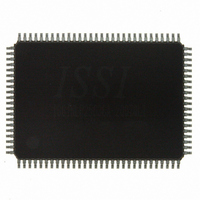
IS61NLP25636A-200TQLI ISSI, Integrated Silicon Solution Inc, IS61NLP25636A-200TQLI Datasheet - Page 27

IS61NLP25636A-200TQLI
Manufacturer Part Number
IS61NLP25636A-200TQLI
Description
IC SRAM 9MBIT 200MHZ 100TQFP
Manufacturer
ISSI, Integrated Silicon Solution Inc
Datasheet
1.IS61NLP25636A-200TQLI-TR.pdf
(37 pages)
Specifications of IS61NLP25636A-200TQLI
Format - Memory
RAM
Memory Type
SRAM - Synchronous
Memory Size
9M (256K x 36)
Speed
200MHz
Interface
Parallel
Voltage - Supply
3.135 V ~ 3.465 V
Operating Temperature
-40°C ~ 85°C
Package / Case
100-TQFP, 100-VQFP
Density
9Mb
Access Time (max)
3.1ns
Sync/async
Synchronous
Architecture
SDR
Clock Freq (max)
200MHz
Operating Supply Voltage (typ)
3.3V
Address Bus
18b
Package Type
TQFP
Operating Temp Range
-40C to 85C
Number Of Ports
4
Supply Current
280mA
Operating Supply Voltage (min)
3.135V
Operating Supply Voltage (max)
3.465V
Operating Temperature Classification
Industrial
Mounting
Surface Mount
Pin Count
100
Word Size
36b
Number Of Words
256K
Lead Free Status / RoHS Status
Lead free / RoHS Compliant
Other names
706-1102
IS61NLP25636A-200TQLI
IS61NLP25636A-200TQLI
Available stocks
Company
Part Number
Manufacturer
Quantity
Price
Company:
Part Number:
IS61NLP25636A-200TQLI
Manufacturer:
ISSI, Integrated Silicon Solution Inc
Quantity:
10 000
Part Number:
IS61NLP25636A-200TQLI
Manufacturer:
ISSI
Quantity:
20 000
Company:
Part Number:
IS61NLP25636A-200TQLI-TR
Manufacturer:
ISSI, Integrated Silicon Solution Inc
Quantity:
10 000
IS61NLP25636A/IS61NVP25636A
IS61NLP51218A/IS61NVP51218A
TAP Electrical Characteristics Over the Operating Range
Notes:
TAP AC ELECTRICAL CHARACTERISTICS
Notes:
1. Both t
2. Test conditions are specified using the load in TAP AC test conditions. t
Integrated Silicon Solution, Inc. — www.issi.com —
Rev. G
07/28/2010
Symbol
V
V
V
V
V
V
I
1. All Voltage referenced to Ground.
2. Overshoot: V
x
oh1
oh2
ol1
ol2
Symbol Parameter
t
f
t
t
t
t
t
t
t
t
t
t
Ih
Il
Tcyc
Tf
Th
Tl
TMSS
TdIS
cS
TMSh
TdIh
ch
TdoV
Tdox
Undershoot: V
Power-up: V
cS
and t
TCK Clock cycle time
TCK Clock frequency
TCK Clock HIGH
TCK Clock LOW
TMS setup to TCK Clock Rise
TDI setup to TCK Clock Rise
Capture setup to TCK Rise
TMS hold after TCK Clock Rise
TDI Hold after Clock Rise
Capture hold after Clock Rise
TCK LOW to TDO valid
TCK LOW to TDO invalid
ch
Ih
Ih
Il
< 2.6V and V
refer to the set-up and hold time requirements of latching data from the boundary scan register.
(AC) ≤ V
(AC)
Parameter
Output HIGH Voltage
Output HIGH Voltage
Output LOW Voltage
Output LOW Voltage
Input HIGH Voltage
Input LOW Voltage
Input Leakage Current
≤
0.5V for t
dd
+1.5V for t
dd
< 2.4V and V
≤
t
Tcyc
≤
t
Tcyc
/2,
ddq
/2,
< 1.4V for t < 200 ms.
(1,2)
1-800-379-4774
(OVER OPERATING RANGE)
Test Conditions
V
I
I
SS
oh
oh
I
I
ol
ol
≤ V I ≤ V
= –2.0 mA
= –100 µA
= 2.0 mA
= 100 µA
r
/t
f
= 1 ns.
(1,2)
ddq
Min.
100
40
40
10
10
10
10
10
10
—
—
0
Max.
10
20
—
—
—
—
—
—
—
—
—
—
Min.
–0.3
–10
1.7
2.1
1.7
—
—
V
dd
Max.
0.7
0.2
0.7
MHz
Unit
—
—
10
ns
ns
ns
ns
ns
ns
ns
ns
ns
ns
ns
+0.3
Units
µA
V
V
V
V
V
V
27


