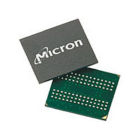
MT46H32M32LFCM-5 IT:A Micron Technology Inc, MT46H32M32LFCM-5 IT:A Datasheet - Page 33

MT46H32M32LFCM-5 IT:A
Manufacturer Part Number
MT46H32M32LFCM-5 IT:A
Description
IC DDR SDRAM 1GBIT 90VFBGA
Manufacturer
Micron Technology Inc
Type
DDR SDRAMr
Specifications of MT46H32M32LFCM-5 IT:A
Format - Memory
RAM
Memory Type
Mobile DDR SDRAM
Memory Size
1G (32M x 32)
Speed
200MHz
Interface
Parallel
Voltage - Supply
1.7 V ~ 1.95 V
Operating Temperature
-40°C ~ 85°C
Package / Case
90-VFBGA
Organization
32Mx32
Density
1Gb
Address Bus
13b
Access Time (max)
6.5/5ns
Maximum Clock Rate
200MHz
Operating Supply Voltage (typ)
1.8V
Package Type
VFBGA
Operating Temp Range
-40C to 85C
Operating Supply Voltage (max)
1.95V
Operating Supply Voltage (min)
1.7V
Supply Current
150mA
Pin Count
90
Mounting
Surface Mount
Operating Temperature Classification
Industrial
Lead Free Status / RoHS Status
Lead free / RoHS Compliant
DESELECT
NO OPERATION
LOAD MODE REGISTER
ACTIVE
PDF: 09005aef82ce3074
1gb_ddr_mobile_sdram_t48m.pdf - Rev. K 07/09 EN
Notes:
Table 15: DM Operation Truth Table
The DESELECT function (CS# HIGH) prevents new commands from being executed by
the device. Operations already in progress are not affected.
The NO OPERATION (NOP) command is used to instruct the selected device to perform
a NOP. This prevents unwanted commands from being registered during idle or wait
states. Operations already in progress are not affected.
The mode registers are loaded via inputs A[0:n]. See mode register descriptions in Stand-
ard Mode Register (page 48) and Extended Mode Register (page 52). The LOAD
MODE REGISTER command can only be issued when all banks are idle, and a subse-
quent executable command cannot be issued until
The ACTIVE command is used to activate a row in a particular bank for a subsequent
access. The values on the BA0 and BA1 inputs select the bank, and the address provided
on inputs A[0:n] selects the row. This row remains active for accesses until a PRE-
CHARGE command is issued to that bank. A PRECHARGE command must be issued
before opening a different row in the same bank.
Name (Function)
Write enable
Write inhibit
1. Used to mask write data; provided coincident with the corresponding data.
2. All states and sequences not shown are reserved and/or illegal.
33
DM
H
L
1Gb: x16, x32 Mobile LPDDR SDRAM
Micron Technology, Inc. reserves the right to change products or specifications without notice.
t
MRD is met.
Valid
DQ
X
©2007 Micron Technology, Inc. All rights reserved.
Commands
Notes
1, 2
1, 2


