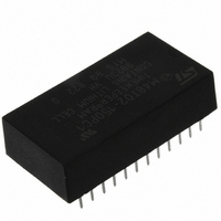
M48Z02-70PC1 STMicroelectronics, M48Z02-70PC1 Datasheet - Page 8

M48Z02-70PC1
Manufacturer Part Number
M48Z02-70PC1
Description
IC NVSRAM 16KBIT 70NS 24DIP
Manufacturer
STMicroelectronics
Specifications of M48Z02-70PC1
Format - Memory
RAM
Memory Type
NVSRAM (Non-Volatile SRAM)
Memory Size
16K (2K x 8)
Speed
70ns
Interface
Parallel
Voltage - Supply
4.75 V ~ 5.5 V
Operating Temperature
0°C ~ 70°C
Package / Case
24-DIP (600 mil) Module
Data Bus Width
8 bit
Organization
2 Kb x 8
Interface Type
Parallel
Access Time
70 ns
Supply Voltage (max)
5.5 V
Supply Voltage (min)
4.75 V
Operating Current
80 mA
Maximum Operating Temperature
70 C
Minimum Operating Temperature
0 C
Mounting Style
Through Hole
Lead Free Status / RoHS Status
Lead free / RoHS Compliant
Other names
497-2868-5
Available stocks
Company
Part Number
Manufacturer
Quantity
Price
Part Number:
M48Z02-70PC1
Manufacturer:
ST
Quantity:
20 000
Operation modes
Figure 4.
Note:
Table 3.
1. Valid for ambient operating temperature: T
2.2
8/22
noted).
Symbol
t
t
t
t
t
t
t
t
t
GHQZ
GLQV
GLQX
EHQZ
AXQX
AVQV
ELQV
ELQX
AVAV
A0-A10
E
G
DQ0-DQ7
READ mode AC waveforms
WRITE enable (W) = high.
READ mode AC characteristics
WRITE mode
The M48Z02/12 is in the WRITE mode whenever W and E are active. The start of a WRITE
is referenced from the latter occurring falling edge of W or E. A WRITE is terminated by the
earlier rising edge of W or E. The addresses must be held valid throughout the cycle. E or W
must return high for a minimum of t
to the initiation of another READ or WRITE cycle. Data-in must be valid t
end of WRITE and remain valid for t
cycles to avoid bus contention; although, if the output bus has been activated by a low on E
and G, a low on W will disable the outputs t
READ cycle time
Address valid to output valid
Chip enable low to output valid
Output enable low to output valid
Chip enable low to output transition
Output enable low to output transition
Chip enable high to output Hi-Z
Output enable high to output Hi-Z
Address transition to output transition
Parameter
tAVQV
tELQX
A
tGLQX
tELQV
= 0 to 70 °C or –40 to 85 °C; V
(1)
tGLQV
Doc ID 2420 Rev 8
EHAX
WHDX
VALID
tAVAV
from chip enable or t
afterward. G should be kept high during WRITE
WLQZ
Min
70
10
5
5
after W falls.
–70
CC
VALID
= 4.75 to 5.5 V or 4.5 to 5.5 V (except where
Max
70
70
35
25
25
M48Z02/M48Z12
Min
150
10
WHAX
tGHQZ
5
5
–150
Max
from WRITE enable prior
150
150
75
35
35
DVWH
Min
200
10
M48Z02, M48Z12
5
5
tAXQX
tEHQZ
–200
prior to the
Max
200
200
80
40
40
AI01330
Unit
ns
ns
ns
ns
ns
ns
ns
ns
ns


