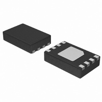
CAT93C66VP2I-GT3 ON Semiconductor, CAT93C66VP2I-GT3 Datasheet - Page 8

CAT93C66VP2I-GT3
Manufacturer Part Number
CAT93C66VP2I-GT3
Description
IC EEPROM 4KB 2MHZ 8-TDFN
Manufacturer
ON Semiconductor
Datasheet
1.CAT93C66VI-GT3.pdf
(15 pages)
Specifications of CAT93C66VP2I-GT3
Format - Memory
EEPROMs - Serial
Memory Type
EEPROM
Memory Size
4K (512 x 8 or 256 x 16)
Speed
2MHz
Interface
Microwire, 3-Wire Serial
Voltage - Supply
1.8 V ~ 5.5 V
Operating Temperature
-40°C ~ 85°C
Package / Case
8-VFDFN Exposed Pad
Lead Free Status / RoHS Status
Lead free / RoHS Compliant
Available stocks
Company
Part Number
Manufacturer
Quantity
Price
Company:
Part Number:
CAT93C66VP2I-GT3
Manufacturer:
TDK
Quantity:
460 000
Erase All
(Chip Select) pin must be deselected for a minimum of
t
clear cycle of all memory locations in the device. The
clocking of the SK pin is not necessary after the device has
entered the self clocking mode. The ready/busy status of the
CAT93C66 can be determined by selecting the device and
polling the DO pin. Once cleared, the contents of all memory
bits return to a logical “1” state.
CSMIN
Upon receiving an ERAL command (Figure 7), the CS
DO
CS
SK
DI
DO
CS
SK
DI
. The falling edge of CS will start the self clocking
1
1
0
0
HIGH−Z
0
0
0
1
1
0
Figure 8. WRAL Instruction Timing
Figure 7. ERAL Instruction Timing
http://onsemi.com
8
Write All
(Chip Select) pin must be deselected for a minimum of
t
clocking data write to all memory locations in the device.
The clocking of the SK pin is not necessary after the device
has entered the self clocking mode. The ready/busy status of
the CAT93C66 can be determined by selecting the device
and polling the DO pin. It is not necessary for all memory
locations to be cleared before the WRAL command is
executed.
CSMIN
D
Upon receiving a WRAL command and data, the CS
N
(Figure 8). The falling edge of CS will start the self
t
SV
D
t
EW
0
STATUS VERIFY
t
CS
BUSY
t
SV
t
EW
READY
STATUS VERIFY
BUSY
t
CSMIN
t
READY
HZ
STANDBY
HIGH−Z
STANDBY
HIGH−Z
t
HZ


