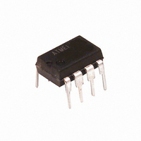
AT25010-10PC Atmel, AT25010-10PC Datasheet

AT25010-10PC
Specifications of AT25010-10PC
Related parts for AT25010-10PC
AT25010-10PC Summary of contents
Page 1
... The AT25010/020/040 is available in space saving 8-lead PDIP and 8-lead JEDEC SOIC packages. The AT25010/020/040 is enabled through the Chip Select pin (CS) and accessed via a 3-wire interface consisting of Serial Data Input (SI), Serial Data Output (SO), and Serial Clock (SCK) ...
Page 2
... Storage Temperature .................................... -65° 150°C Voltage on Any Pin with Respect to Ground ....................................-1. 7.0V Maximum Operating Voltage .......................................... 6.25V DC Output Current........................................................ 5.0 mA Block Diagram AT25010/020/040 2 *NOTICE: Stresses beyond those listed under “Absolute Maximum Ratings” may cause permanent dam- age to the device. This is a stress rating only and ...
Page 3
... 5. MHz Open, Read MHz Open -100 µA OH AT25010/020/040 = +5.0V (unless otherwise noted). CC Max Units Conditions OUT +2.7V to +5.5V +2.7V to +5. Min Max Units 2.7 5.5 4.5 5.5 3.0 6 -0.6 3.0 -0.6 3 ...
Page 4
... Hold to Output High Output Disable Time DIS t Write Cycle Time WC (1) Endurance 5.0V Page Mode Note: 1. This parameter is characterized and is not 100% tested. AT25010/020/040 4 = -40°C to +85° Specified TTL Gate and AI CC Voltage Min 4.5 - 5.5 0 2.7 - 5.5 0 4.5 - 5.5 2 ...
Page 5
... WRITE PROTECT: The write protect pin (WP) will allow normal read/write operations when held high. When the WP pin is brought low, all write operations are inhibited. WP going low while CS is still low will interrupt a write to the AT25010/020/040. If the internal write cycle has already been initiated, WP going low will have no effect on any write operation. 0606M– ...
Page 6
... The AT25010/020/040 is designed to interface directly with the synchronous serial peripheral interface (SPI) of the 6805 and 68HC11 series of microcontrollers. The AT25010/020/040 utilizes an 8-bit instruction register. The list of instructions and their operation codes are contained in Table 1. All instructions, addresses, and data are transferred with the MSB first and start with a high-to-low CS transition. ...
Page 7
... Table 3. Read Status Register Bit Definition WRITE STATUS REGISTER (WRSR): The WRSR instruction allows the user to select one of four levels of protection. The AT25010/020/040 is divided into four array seg- ments. Top quarter (1/4), Top half (1/2), or all of the memory segments can be protected. Any of the data within any selected segment will therefore be READ only. The block write protection levels and corresponding status register control bits are shown in Table 4 ...
Page 8
... Bit the WRITE cycle has ended. Only the READ STATUS REGISTER instruction is enabled during the WRITE programming cycle. The AT25010/020/040 is capable of an 8-byte PAGE WRITE operation. After each byte of data is received, the three low order address bits are internally incremented by one; ...
Page 9
... Timing Diagrams Synchronous Data Timing (for mode CSS V IH SCK HI WREN Timing WRDI Timing 0606M–SEEPR–06/ VALID AT25010/020/040 CSH DIS HI-Z 9 ...
Page 10
... RDSR Timing CS 0 SCK SI HIGH IMPEDANCE SO WRSR Timing CS 0 SCK SI HIGH IMPEDANCE SO READ Timing AT25010/020/040 INSTRUCTION 7 MSB INSTRUCTION DATA OUT DATA 0606M–SEEPR–06/03 ...
Page 11
... WRITE Timing SCK INSTRUCTION SI HIGH IMPEDANCE SO HOLD Timing CS SCK HOLD SO 0606M–SEEPR–06/ BYTE ADDRESS 9TH BIT OF ADDRESS AT25010/020/040 23 DATA ...
Page 12
... AT25010 Ordering Information Ordering Code AT25010-10PI-2.7 AT25010N-10SI-2.7 Note: For 2.7V devices used in the 4.5V to 5.5V range, please refer to performance values in the AC and DC Characteristics tables. 8P3 8-lead, 0.300" Wide, Plastic Dual Inline Package (PDIP) 8S1 8-lead, 0.150" Wide, Plastic Gull Wing Small Outline Package (JEDEC SOIC) -2 ...
Page 13
... For 2.7V devices used in the 4.5V to 5.5V range, please refer to performance values in the AC and DC Characteristics tables. 8P3 8-lead, 0.300" Wide, Plastic Dual Inline Package (PDIP) 8S1 8-lead, 0.150" Wide, Plastic Gull Wing Small Outline Package (JEDEC SOIC) -2.7 Low Voltage (2.7V to 5.5V) 0606M–SEEPR–06/03 Package 8P3 8S1 Package Type Options AT25010/020/040 Operation Range Industrial (- ...
Page 14
... For 2.7V devices used in the 4.5V to 5.5V range, please refer to performance values in the AC and DC Characteristics tables. 8P3 8-lead, 0.300" Wide, Plastic Dual Inline Package (PDIP) 8S1 8-lead, 0.150" Wide, Plastic Gull Wing Small Outline Package (JEDEC SOIC) -2.7 Low Voltage (2.7V to 5.5V) AT25010/020/040 14 Package 8P3 8S1 Package Type Options ...
Page 15
... Dambar protrusions. Dambar protrusions shall not exceed 0.010 (0.25 mm). 2325 Orchard Parkway San Jose, CA 95131 R 0606M–SEEPR–06/ TITLE 8P3, 8-lead, 0.300" Wide Body, Plastic Dual In-line Package (PDIP) AT25010/020/040 End View COMMON DIMENSIONS (Unit of Measure = inches) MIN SYMBOL NOM MAX A 0.210 A2 0.115 0.130 ...
Page 16
... Side View End View Note: This drawing is for general information only. Refer to JEDEC Drawing MS-012 for proper dimensions, tolerances, datums, etc. 2325 Orchard Parkway San Jose, CA 95131 R AT25010/020/040 TITLE 8S1, 8-lead (0.150" Wide Body), Plastic Gull Wing Small Outline (JEDEC SOIC) ...
Page 17
... No licenses to patents or other intellectual property of Atmel are granted by the Company in connection with the sale of Atmel products, expressly or by implication. Atmel’s products are not authorized for use as critical components in life support devices or systems. ...


