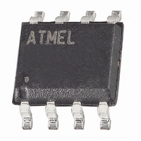
AT25040N-10SC Atmel, AT25040N-10SC Datasheet - Page 7

AT25040N-10SC
Manufacturer Part Number
AT25040N-10SC
Description
IC EEPROM 4KBIT 2.1MHZ 8SOIC
Manufacturer
Atmel
Datasheet
1.AT25010-10PC.pdf
(17 pages)
Specifications of AT25040N-10SC
Format - Memory
EEPROMs - Serial
Memory Type
EEPROM
Memory Size
4K (512 x 8)
Speed
2.1MHz
Interface
SPI, 3-Wire Serial
Voltage - Supply
4.5 V ~ 5.5 V
Operating Temperature
0°C ~ 70°C
Package / Case
8-SOIC (3.9mm Width)
Lead Free Status / RoHS Status
Contains lead / RoHS non-compliant
Available stocks
Company
Part Number
Manufacturer
Quantity
Price
Company:
Part Number:
AT25040N-10SC-2.7
Manufacturer:
ATMEL
Quantity:
1 506
Part Number:
AT25040N-10SC2.7
Manufacturer:
ATMEL/爱特梅尔
Quantity:
20 000
0606M–SEEPR–06/03
WRITE ENABLE (WREN): The device will power up in the write disable state when V
is applied. All programming instructions must therefore be preceded by a Write Enable
instruction. The WP pin must be held high during a WREN instruction.
WRITE DISABLE (WRDI): To protect the device against inadvertent writes, the Write
Disable instruction disables all programming modes. The WRDI instruction is indepen-
dent of the status of the WP pin.
READ STATUS REGISTER (RDSR): The Read Status Register instruction provides
access to the status register. The READY/BUSY and Write Enable status of the device
can be determined by the RDSR instruction. Similarly, the Block Write Protection bits
indicate the extent of protection employed. These bits are set by using the WRSR
instruction.
Table 2. Status Register Format
Table 3. Read Status Register Bit Definition
WRITE STATUS REGISTER (WRSR): The WRSR instruction allows the user to select
one of four levels of protection. The AT25010/020/040 is divided into four array seg-
ments. Top quarter (1/4), Top half (1/2), or all of the memory segments can be
protected. Any of the data within any selected segment will therefore be READ only. The
block write protection levels and corresponding status register control bits are shown in
Table 4.
The two bits, BP1 and BP0 are nonvolatile cells that have the same properties and func-
tions as the regular memory cells (e.g. WREN, t
Table 4. Block Write Protect Bits
Bit
Bit 0 (RDY)
Bit 1 (WEN)
Bit 2 (BP0)
Bit 3 (BP1)
Bits 4-7 are 0s when device is not in an internal write cycle.
Bits 0-7 are 1s during an internal write cycle.
Bit 7
X
Level
1 (1/4)
2 (1/2)
3 (All)
0
Bit 6
X
Status Register Bits
BP1
0
0
1
1
Bit 5
X
Definition
Bit 0 = 0 (RDY) indicates the device is READY. Bit 0 = 1 indicates the
write cycle is in progress.
Bit 1 = 0 indicates the device is not WRITE ENABLED. Bit 1 = 1 indicates
the device is WRITE ENABLED.
See Table 4.
See Table 4.
BP0
0
1
0
1
Bit 4
X
AT25010
60-7F
40-7F
00-7F
None
Bit 3
BP1
WC
, RDSR).
Array Addresses Protected
AT25010/020/040
Bit 2
BP0
AT25020
C0-FF
80-FF
00-FF
None
Bit 1
WEN
AT25040
180-1FF
100-1FF
000-1FF
None
Bit 0
RDY
CC
7


