AT28LV010-20JC Atmel, AT28LV010-20JC Datasheet
AT28LV010-20JC
Specifications of AT28LV010-20JC
Available stocks


Related parts for AT28LV010-20JC


AT28LV010-20JC Summary of contents
Page 1
... Commercial and Industrial Temperature Ranges Description The AT28LV010 is a high-performance 3-volt only Electrically Erasable and Program- mable Read Only Memory. Its 1 megabit of memory is organized as 131,072 words by 8 bits. Manufactured with Atmel’s advanced nonvolatile CMOS technology, the device offers access times to 200 ns with power dissipation of just 54 mW. When the device is deselected, the CMOS standby current is less than 20 µ ...
Page 2
... The AT28LV010 is accessed like a Static RAM for the read or write cycle without the need for external components. The device contains a 128-byte page register to allow writ- ing 128 bytes simultaneously. During a write cycle, the address and 1 to 128 bytes of data are internally latched, freeing the address and data bus for other opera- tions ...
Page 3
... high. This dual- line control gives designers flexibility in preventing bus con- tention in their system. WRITE: The write operation of the AT28LV010 allows 1 to 128 bytes of data to be written into the device during a sin- gle internal programming period. Each write operation must be preceded by the software data protection (SDP) com- mand sequence ...
Page 4
... IH V Output Low Voltage OL V Output High Voltage OH AT28LV010 4 AT28LV010-20 0°C - 70°C -40°C - 85° Condition I/O CC Com 0. Ind MHz mA 3.6V OUT 1 -100 3. AT28LV010-25 0°C - 70°C -40°C - 85°C 3.3V 10 OUT High High Z Min Max Units 0.8 V 2.0 V 0.45 V 2.4 V ...
Page 5
... OUT Note: 1. This parameter is characterized and is not 100% tested after the address transition without impact on t ACC after the falling edge of CE without impact pF). L Output Test Load Max 6 12 AT28LV010-20 AT28LV010-25 Min Max Min 200 200 ACC after an address change ...
Page 6
... Chip Select Set-up Time CS t Chip Select Hold Time CH t Write Pulse Width ( Data Set-up Time Data, OE Hold Time DH OEH Note: 1. All write operations must be preceded by the SDP command sequence. AC Write Waveforms WE Controlled CE Controlled AT28LV010 6 (1) Min Max Units 0 ns 100 200 ns 100 ...
Page 7
Software Protected Write Characteristics Symbol Parameter t Write Cycle Time WC t Address Set-up Time AS t Address Hold Time AH t Data Set-up Time DS t Data Hold Time DH t Write Pulse Width WP t Byte Load Cycle ...
Page 8
... These parameters are characterized and not 100% tested. 2. See AC Read Characteristics Toggle Bit Waveforms Notes: 1. Toggling either both OE and CE will operate toggle bit. 2. Beginning and ending state of I/O6 will vary. 3. Any address location may be used but the address should not vary. AT28LV010 8 (1) (1) Min Typ Max ...
Page 9
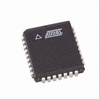
... Reference Section: Parallel EEPROM Die Products 32J 32-Lead, Plastic J-Leaded Chip Carrier (PLCC) 32P6 32-Lead, 0.600” Wide, Plastic Dual Inline Package (PDIP) 32T 32-Lead, Plastic Thin Small Outline Package (TSOP) Ordering Code AT28LV010-20JC AT28LV010-20PC AT28LV010-20TC AT28LV010-20JI AT28LV010-20PI AT28LV010-20TI AT28LV010-25JC AT28LV010-25PC ...
Page 10
... REF 8.20(.323) 7.80(.307) 0.15(.006) 0.05(.002 REF 0.70(.028) 0.50(.020) *Controlling dimension: millimeters AT28LV010 10 32P6, 32-Lead, 0.600” Wide, Plastic Dual Inline Package (PDIP) Dimensions in Inches and (Millimeters) .025(.635 .012(.305) .008(.203) .530(13.5 .490(12.4 ...
Page 11
11 ...
Page 12
... No licenses to patents or other intellectual prop Atmel are granted by the Company in connection with the sale of Atmel products, expressly or by implication. Atmel’s products are not authorized for use as critical components in life suppor t devices or systems. ...