AT29C020-12PC Atmel, AT29C020-12PC Datasheet - Page 5
AT29C020-12PC
Manufacturer Part Number
AT29C020-12PC
Description
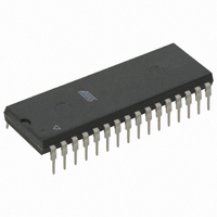
IC FLASH 2MBIT 120NS 32DIP
Manufacturer
Atmel
Datasheet
1.AT29C020-12JU.pdf
(17 pages)
Specifications of AT29C020-12PC
Format - Memory
FLASH
Memory Type
FLASH
Memory Size
2M (256K x 8)
Speed
120ns
Interface
Parallel
Voltage - Supply
4.5 V ~ 5.5 V
Operating Temperature
0°C ~ 70°C
Package / Case
32-DIP (0.600", 15.24mm)
Lead Free Status / RoHS Status
Contains lead / RoHS non-compliant
Available stocks
Company
Part Number
Manufacturer
Quantity
Price
Company:

Part Number:
AT29C020-12PC
Manufacturer:
ATMEL
Quantity:
5 510
Part Number:
AT29C020-12PC
Manufacturer:
AMD
Quantity:
20 000


4.9
4.10
4.10.1
5. Absolute Maximum Ratings*
0291S–FLASH–11/08
Temperature Under Bias ............................... -55C to +125C
Storage Temperature..................................... -65C to +150C
All Input Voltages (including NC Pins)
with Respect to Ground ...................................-0.6V to +6.25V
All Output Voltages
with Respect to Ground .............................-0.6V to V
Voltage on OE
with Respect to Ground ...................................-0.6V to +13.5V
Optional Chip Erase Mode
Boot Block Programming Lockout
Boot Block Lockout Detection
The entire device can be erased by using a 6-byte software code. Please see Software Chip
Erase application note for details.
The AT29C020 has two designated memory blocks that have a programming lockout feature.
This feature prevents programming of data in the designated block once the feature has been
enabled. Each of these blocks consists of 8K bytes; the programming lockout feature can be set
independently for either block. While the lockout feature does not have to be activated, it can be
activated for either or both blocks.
These two 8K memory sections are referred to as boot blocks. Secure code which will bring up a
system can be contained in a boot block. The AT29C020 blocks are located in the first 8K bytes
of memory and the last 8K bytes of memory. The boot block programming lockout feature can
therefore support systems that boot from the lower addresses of memory or the higher
addresses. Once the programming lockout feature has been activated, the data in that block can
no longer be erased or programmed; data in other memory locations can still be changed
through the regular programming methods. To activate the lockout feature, a series of seven
program commands to specific addresses with specific data must be performed. Please see
Boot Block Lockout Feature Enable Algorithm.
If the boot block lockout feature has been activated on either block, the chip erase function will
be disabled.
A software method is available to determine whether programming of either boot block section is
locked out. See Software Product Identification Entry and Exit sections. When the device is in
the software product identification mode, a read from location 00002H will show if programming
the lower address boot block is locked out while reading location 3FFF2H will do so for the upper
boot block. If the data is FE, the corresponding block can be programmed; if the data is FF, the
program lockout feature has been activated and the corresponding block cannot be pro-
grammed. The software product identification exit mode should be used to return to standard
operation.
CC
+ 0.6V
*NOTICE:
Stresses beyond those listed under “Absolute
Maximum Ratings” may cause permanent dam-
age to the device. This is a stress rating only and
functional operation of the device at these or any
other conditions beyond those indicated in the
operational sections of this specification is not
implied. Exposure to absolute maximum rating
conditions for extended periods may affect
device reliability.
AT29C020
5
Related parts for AT29C020-12PC
Image
Part Number
Description
Manufacturer
Datasheet
Request
R

Part Number:
Description:
Manufacturer:
ATMEL Corporation
Datasheet:

Part Number:
Description:
IC FLASH MEM 2MBIT 120NS 32TSOP
Manufacturer:
Atmel
Datasheet:

Part Number:
Description:
IC FLASH 2MBIT 70NS 32PLCC
Manufacturer:
Atmel
Datasheet:
Part Number:
Description:
IC FLASH 2MBIT 120NS 32PLCC
Manufacturer:
Atmel
Datasheet:
Part Number:
Description:
IC FLASH 2MBIT 120NS 32TSOP
Manufacturer:
Atmel
Datasheet:
Part Number:
Description:
IC FLASH 2MBIT 120NS 32TSOP
Manufacturer:
Atmel
Datasheet:

Part Number:
Description:
IC FLASH 2MBIT 150NS 32DIP
Manufacturer:
Atmel
Datasheet:
Part Number:
Description:
IC FLASH 2MBIT 150NS 32TSOP
Manufacturer:
Atmel
Datasheet:
Part Number:
Description:
IC FLASH 2MBIT 90NS 32PLCC
Manufacturer:
Atmel
Datasheet:
Part Number:
Description:
IC FLASH 2MBIT 90NS 32DIP
Manufacturer:
Atmel
Datasheet:
Part Number:
Description:
IC FLASH 2MBIT 90NS 32DIP
Manufacturer:
Atmel
Datasheet:
Part Number:
Description:
IC FLASH 2MBIT 90NS 32TSOP
Manufacturer:
Atmel
Datasheet:
Part Number:
Description:
IC FLASH 2MBIT 70NS 32DIP
Manufacturer:
Atmel
Datasheet:
Part Number:
Description:
IC FLASH 2MBIT 70NS 32DIP
Manufacturer:
Atmel
Datasheet: