AT29C040A-10PC Atmel, AT29C040A-10PC Datasheet - Page 3
AT29C040A-10PC
Manufacturer Part Number
AT29C040A-10PC
Description
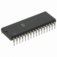
IC FLASH 4MBIT 100NS 32DIP
Manufacturer
Atmel
Datasheet
1.AT29C040A-12PC.pdf
(17 pages)
Specifications of AT29C040A-10PC
Format - Memory
FLASH
Memory Type
FLASH
Memory Size
4M (512K x 8)
Speed
100ns
Interface
Parallel
Voltage - Supply
4.5 V ~ 5.5 V
Operating Temperature
0°C ~ 70°C
Package / Case
32-DIP (0.600", 15.24mm)
Lead Free Status / RoHS Status
Contains lead / RoHS non-compliant
Other names
AT29C040A10PC
Available stocks
Company
Part Number
Manufacturer
Quantity
Price
Company:

Part Number:
AT29C040A-10PC
Manufacturer:
SIEMENS
Quantity:
6 264


3. Block Diagram
4. Device Operation
4.1
4.2
4.3
4.4
0333L–FLASH–9/08
Read
Byte Load
Program
Software Data Protection
The AT29C040A is accessed like an EPROM. When CE and OE are low and WE is high, the
data stored at the memory location determined by the address pins is asserted on the outputs.
The outputs are put in the high impedance state whenever CE or OE is high. This dual-line con-
trol gives designers flexibility in preventing bus contention.
Byte loads are used to enter the 256 bytes of a sector to be programmed or the software codes
for data protection. A byte load is performed by applying a low pulse on the WE or CE input with
CE or WE low (respectively) and OE high. The address is latched on the falling edge of CE or
WE, whichever occurs last. The data is latched by the first rising edge of CE or WE.
The device is reprogrammed on a sector basis. If a byte of data within a sector is to be changed,
data for the entire sector must be loaded into the device. Any byte that is not loaded during the
programming of its sector will be erased to read FFH. Once the bytes of a sector are loaded into
the device, they are simultaneously programmed during the internal programming period. After
the first data byte has been loaded into the device, successive bytes are entered in the same
manner. Each new byte to be programmed must have its high to low transition on WE (or CE)
within 150 s of the low to high transition of WE (or CE) of the preceding byte. If a high to low
transition is not detected within 150 s of the last low to high transition, the load period will end
and the internal programming period will start. A8 to A18 specify the sector address. The sector
address must be valid during each high to low transition of WE (or CE). A0 to A7 specify the byte
address within the sector. The bytes may be loaded in any order; sequential loading is not
required. Once a programming operation has been initiated, and for the duration of t
operation will effectively be a polling operation.
A software controlled data protection feature is available on the AT29C040A. Once the software
protection is enabled a software algorithm must be issued to the device before a program may
AT29C040A
WC
, a read
3
Related parts for AT29C040A-10PC
Image
Part Number
Description
Manufacturer
Datasheet
Request
R

Part Number:
Description:
AT29C040A-124-Megabit 512K x 8 5-volt Only 256-Byte Sector CMOS Flash Memory
Manufacturer:
ATMEL Corporation
Datasheet:
Part Number:
Description:
Manufacturer:
ATMEL Corporation
Datasheet:

Part Number:
Description:
IC FLASH 4MBIT 120NS 32DIP
Manufacturer:
Atmel
Datasheet:
Part Number:
Description:
IC FLASH 4MBIT 120NS 32DIP
Manufacturer:
Atmel
Datasheet:

Part Number:
Description:
IC FLASH 4MBIT 120NS 32TSOP
Manufacturer:
Atmel
Datasheet:
Part Number:
Description:
IC FLASH 4MBIT 100NS 32TSOP
Manufacturer:
Atmel
Datasheet:
Part Number:
Description:
IC FLASH 4MBIT 150NS 32DIP
Manufacturer:
Atmel
Datasheet:

Part Number:
Description:
IC FLASH 4MBIT 120NS 32PLCC
Manufacturer:
Atmel
Datasheet:
Part Number:
Description:
IC FLASH 4MBIT 120NS 32PLCC
Manufacturer:
Atmel
Datasheet:
Part Number:
Description:
IC FLASH 4MBIT 90NS 32PLCC
Manufacturer:
Atmel
Datasheet:
Part Number:
Description:
IC FLASH 4MBIT 90NS 32DIP
Manufacturer:
Atmel
Datasheet:
Part Number:
Description:
IC FLASH 4MBIT 90NS 32DIP
Manufacturer:
Atmel
Datasheet:
Part Number:
Description:
IC FLASH 4MBIT 90NS 32TSOP
Manufacturer:
Atmel
Datasheet:
Part Number:
Description:
IC FLASH 4MBIT 120NS 32PLCC
Manufacturer:
Atmel
Datasheet:
Part Number:
Description:
IC FLASH 4MBIT 120NS 32TSOP
Manufacturer:
Atmel
Datasheet: