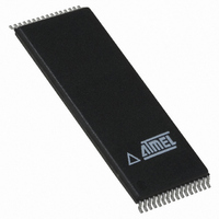
AT49F002T-12TC Atmel, AT49F002T-12TC Datasheet

AT49F002T-12TC
Specifications of AT49F002T-12TC
Related parts for AT49F002T-12TC
AT49F002T-12TC Summary of contents
Page 1
... A15 11 22 A12 2-megabit (256K x 8) 5-volt Only Flash Memory AT49F002 AT49F002N AT49F002T AT49F002NT Not Recommended for New Design Contact Atmel to discuss the latest design in trends and options OE A10 CE I/O7 I/O6 I/O5 I/O4 I/O3 GND I/O2 I/O1 I/ Rev. 1017D–10/ ...
Page 2
... The device is erased by executing the erase command sequence; the device internally controls the erase opera- tions. There are two 8K byte parameter block sections and two main memory blocks. The device has the capability to protect the data in the boot block; this feature is enabled by a command sequence. ...
Page 3
... ERASURE: Before a byte can be reprogrammed, the main memory block or parameter block which contains the byte must be erased. The erased state of the memory bits is a logical “1”. The entire device can be erased at one time by using a 6-byte software code. The software chip erase ...
Page 4
... This feature is not available on the AT49F002N(T). AT49F002(N)(T) 4 PRODUCT IDENTIFICATION: The product identification mode identifies the device and manufacturer as Atmel. It may be accessed by hardware or software operation. The hardware operation mode can be used by an external pro- grammer to identify the correct programming algorithm for the Atmel product. ...
Page 5
... SA = 38000 to 39FFF for PARAMETER BLOCK 20000 to 37FFF for MAIN MEMORY ARRAY BLOCK 1 This command will erase - PB1, PB2 and MMB1 SA = 00000 to IFFFF for MAIN MEMORY ARRAY BLOCK 2 Absolute Maximum Ratings* Temperature Under Bias................................ -55°C to +125°C Storage Temperature ..................................... -65°C to +150°C ...
Page 6
DC and AC Operating Range Com. Operating Temperature (Case) Ind. V Power Supply CC Operating Modes Mode CE Read V IL (2) Program/Erase V IL Standby/Write Inhibit Program Inhibit X Output Disable X Reset X Product Identification ...
Page 7
AC Read Characteristics Symbol Parameter t Address to Output Delay ACC ( Output Delay CE ( Output Delay OE (3)( Output Float DF Output Hold from OE ...
Page 8
AC Byte Load Characteristics Symbol Parameter Address, OE Set-up Time AS OES t Address Hold Time AH t Chip Select Set-up Time CS t Chip Select Hold Time CH t Write Pulse Width (WE or CE) WP ...
Page 9
Program Cycle Characteristics Symbol Parameter t Byte Programming Time BP t Address Set-up Time AS t Address Hold Time AH t Data Set-up Time DS t Data Hold Time DH t Write Pulse Width WP t Write Pulse Width High ...
Page 10
Data Polling Characteristics Symbol Parameter t Data Hold Time Hold Time OEH ( Output Delay OE t Write Recovery Time WR Notes: 1. These parameters are characterized and not 100% tested. 2. See t ...
Page 11
Software Product Identification Entry LOAD DATA AA TO ADDRESS 5555 LOAD DATA 55 TO ADDRESS 2AAA LOAD DATA 90 TO ADDRESS 5555 ENTER PRODUCT IDENTIFICATION (2)(3)(5) MODE Software Product Identification Exit OR LOAD DATA AA TO ADDRESS 5555 LOAD DATA ...
Page 12
AT49F002 Ordering Information I (mA ACC (ns) Active Standby 55 50 0 0 0.1 50 0.3 120 50 0.1 50 0.3 32J 32-lead, Plastic J-leaded Chip Carrier Package (PLCC) 32P6 ...
Page 13
AT49F002N Ordering Information I (mA ACC (ns) Active Standby 55 50 0 0 0.1 50 0.3 120 50 0.1 50 0.3 32J 32-lead, Plastic J-leaded Chip Carrier Package (PLCC) 32P6 ...
Page 14
... AT49F002T-90JC 32J AT49F002T-90PC 32P6 AT49F002T-90TC 32T AT49F002T-90VC 32V AT49F002T-90JI 32J AT49F002T-90PI 32P6 AT49F002T-90TI 32T AT49F002T-90VI 32V AT49F002T-12JC 32J AT49F002T-12PC 32P6 AT49F002T-12TC 32T AT49F002T-12VC 32V AT49F002T-12JI 32J AT49F002T-12PI 32P6 AT49F002T-12TI 32T AT49F002T-12VI 32V Package Type Operation Range Commercial ( Industrial (- Commercial ( Industrial ...
Page 15
AT49F002NT Ordering Information I (mA ACC (ns) Active Standby 55 50 0 0 0.1 50 0.3 120 50 0.1 50 0.3 32J 32-lead, Plastic J-leaded Chip Carrier Package (PLCC) 32P6 ...
Page 16
Packaging Information 32J, 32-lead, Plastic J-leaded Chip Carrier (PLCC) Dimensions in Inches and (Millimeters) JEDEC STANDARD MS-016 AE .045(1.14) X 45˚ PIN NO. 1 IDENTIFY .553(14.0) .547(13.9) .032(.813) .595(15.1) .026(.660) .585(14.9) .050(1.27) TYP .300(7.62) REF .430(10.9) .390(9.90) AT CONTACT POINTS ...
Page 17
... No licenses to patents or other intellectual prop- erty of Atmel are granted by the Company in connection with the sale of Atmel products, expressly or by implication. Atmel’s products are not authorized for use as critical components in life suppor t devices or systems. ...


